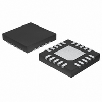
MAX3272AETP+ Maxim Integrated Products, MAX3272AETP+ Datasheet - Page 3

MAX3272AETP+
Manufacturer Part Number
MAX3272AETP+
Description
IC AMP LIMITING 20-TQFN
Manufacturer
Maxim Integrated Products
Type
Limiting Amplifierr
Datasheet
1.MAX3272AETP.pdf
(14 pages)
Specifications of MAX3272AETP+
Applications
Optical Networks
Mounting Type
Surface Mount
Package / Case
20-TQFN Exposed Pad
Input Voltage Range (max)
1200 mV
Operating Supply Voltage
3.3 V
Supply Current
33 mA
Operating Temperature Range
- 40 C to + 85 C
Mounting Style
SMD/SMT
Power Dissipation
1100 mW
Amplifier Type
Low Power
Supply Voltage Range
3V To 3.6V
Amplifier Case Style
TQFN
No. Of Pins
20
Termination Type
SMD
Supply Voltage Min
3V
Rohs Compliant
Yes
Filter Terminals
SMD
Lead Free Status / RoHS Status
Lead free / RoHS Compliant
ELECTRICAL CHARACTERISTICS (continued)
(V
Note 1: Dice are designed and guaranteed from -40°C to +85°C but are tested only at T
Note 2: Supply current measurement excludes the current of the CML output stage (16mA typical). See Figure 1, Power-Supply
Note 3: Guaranteed by design and characterization.
Note 4: Input edge speed is controlled using 4-pole, lowpass Bessel filters with bandwidth approximately 75% of the maximum
Note 5: Deterministic jitter is measured with a K28.5 pattern (0011 1110 1011 0000 0101). Deterministic jitter is the peak-to-peak
Note 6: Random jitter is measured with the minimum input signal. For Fibre Channel and Gigabit Ethernet applications, the peak-
Note 7: Power-supply noise rejection (PSNR) is calculated by the equation PSNR = 20log (∆V
Note 8: Hysteresis is defined as: 20
Note 9: Response time to a 10dB change in input power. For the specification guaranteed, the power is assumed to switch back
Note 10: All power-detect AC parameters are guaranteed with a 2
(V
High LOS Deassert Level
LOS Output High Voltage
LOS Output Low Voltage
Squelch Input Current
CC
CC
1000
950
900
850
800
750
700
650
600
= +3.0V to +3.6V, T
= +3.3V, T
0
PARAMETER
Current Measurement.
data rate.
deviation from ideal time crossings, measured at the zero-level crossings of the differential output per ANSI X3.230, Annex A.
to-peak random jitter is 14.1 times the RMS random jitter.
change in differential output voltage due to the power-supply noise, ∆V
Frequency in the Typical Operating Characteristics.
and forth between two levels (separated by 10dB and equidistant from assert and deassert levels) outside of the two
hysteresis thresholds.
10
vs. INPUT AMPLITUDE
OUTPUT AMPLITUDE
A
= +25°C, unless otherwise noted.)
20
V
_______________________________________________________________________________________
IN
(mV
LEVEL = OPEN
LEVEL = GND
A
P-P
= -40°C to +85°C. Typical values are at V
30
)
40
SYMBOL
✕
50
log(V
LOS-DEASSERT
R
Sinking 30µA
Sourcing 1.2mA
70
65
60
55
50
45
40
35
30
25
20
TH
-40
= 80Ω (Notes 3, 10)
vs. AMBIENT TEMPERATURE
-15
+3.3V, 2.5Gbps Low-Power
/V
AMBIENT TEMPERATURE (°C)
LOS-ASSERT
SUPPLY CURRENT
CONDITIONS
10
23
CC
- 1 PRBS, 2.5Gbps input, with the longest possible run of 80CID.
Typical Operating Characteristics
= +3.3V and T
35
).
60
Limiting Amplifiers
CC
. See Power-Supply Noise Rejection vs.
85
A
= +25°C, unless otherwise noted.)
A
= +25°C.
20
18
16
14
12
10
CC
8
6
4
2
0
1
MIN
/(∆V
2.4
OUT
DETERMINISTIC JITTER
vs. INPUT AMPLITUDE
INPUT AMPLITUDE (mV
10
)), where ∆V
TYP
73
100
124.7
MAX
400
0.4
OUT
1000
P-P
is the
)
UNITS
mV
µA
V
V
P-P
10,000
3


