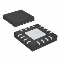
MAX9715ETE+ Maxim Integrated Products, MAX9715ETE+ Datasheet - Page 10

MAX9715ETE+
Manufacturer Part Number
MAX9715ETE+
Description
IC AMP AUDIO PWR 2.8W D 16TQFN
Manufacturer
Maxim Integrated Products
Type
Class Dr
Datasheet
1.MAX9715ETE.pdf
(13 pages)
Specifications of MAX9715ETE+
Output Type
2-Channel (Stereo)
Max Output Power X Channels @ Load
2.8W x 2 @ 4 Ohm
Voltage - Supply
4.5 V ~ 5.5 V
Features
Depop, Short-Circuit and Thermal Protection, Shutdown
Mounting Type
Surface Mount
Package / Case
16-TQFN Exposed Pad
Product
Class-D
Output Power
2.8 W
Thd Plus Noise
0.06 %
Operating Supply Voltage
5 V
Supply Current
12.8 mA
Maximum Power Dissipation
1666 mW
Maximum Operating Temperature
+ 85 C
Mounting Style
SMD/SMT
Minimum Operating Temperature
- 40 C
Supply Voltage (max)
5.5 V
Supply Voltage (min)
4.5 V
Amplifier Class
D
No. Of Channels
2
Supply Voltage Range
4.5V To 5.5V
Load Impedance
4ohm
Operating Temperature Range
-40°C To +85°C
Amplifier Case Style
TQFN
Rohs Compliant
Yes
Lead Free Status / RoHS Status
Lead free / RoHS Compliant
2.8W, Low-EMI, Stereo, Filterless Class D
Audio Amplifier
Proper layout and grounding are essential for optimum
performance. Use large traces for the power-supply
inputs and amplifier outputs to minimize losses due to
parasitic trace resistance. Large traces also aid in moving
heat away from the package. Proper grounding improves
audio performance, minimizes crosstalk between chan-
nels, and prevents any switching noise from coupling into
the audio signal. Route ground return paths that carry
switching transients to power ground (PGND). Keep high-
current return paths that connect to PGND short and
route them away from analog ground (GND) and any
traces or components in the audio input signal path. Use
a star connection to connect GND and PGND together at
one point on the PC board.
Bypass each PV
Bypass V
capacitor between V
capacitors as close to the MAX9715 as possible.
Use large, low-resistance output traces. Current drawn
from the output increases as load impedance decreases.
High-output-trace resistance decreases the power deliv-
ered to the load. For example, when compared to a 0Ω
trace, a 100mΩ trace reduces the power delivered to a
4Ω load from 2.1W to 2.0W. Large output, supply, and
GND traces decrease the thermal impedance of the cir-
cuit and allow more heat to be radiated from the MAX9715
to the air.
The MAX9715 thin QFN-EP package features an
exposed thermal pad on its underside. This pad lowers
the package’s thermal impedance by providing a direct-
10
______________________________________________________________________________________
DD
to GND with a 0.1μF capacitor. Place a bulk
DD
with a 0.1μF capacitor to PGND.
DD
Supply Bypassing, Layout,
and PGND. Place the bypass
and Grounding
heat conduction path from the die to the PC board.
Connect the exposed thermal pad to an electrically iso-
lated pad of copper. A bigger pad area provides better
thermal performance. Connect EP to GND if PC board
layout rules do not allow for isolated pads of copper. If
EP is connected to GND, ensure that high-current return
paths do not flow through EP.
The Typical Application Circuit shows the MAX9715
configured as a mid-/high-frequency amplifier and the
MAX9713 is configured as a mono bass amplifier.
Capacitors C1 and C2 set the highpass cutoff frequen-
cy according to the following equation:
where R
C1 = C2. The 10μF capacitors on the output of the
MAX9715 ensure a two-pole roll-off with the 5Ω load
shown.
The stereo signal is summed to a mono signal and then
sent to a two-pole lowpass filter. The filtered signal is
then amplified by the MAX9713. The passband gain of
the lowpass filter, for coherent left and right signals is
(-2 x R3) / R1, where R1 = R2. The cutoff frequency of
the lowpass filter is set by the following equation:
IN
is the input resistance of the MAX9715 and
f
=
2
1
π
f
×
=
2
C
π
3
×
×
R
1
C
IN
Biamp Configuration
4
×
1
×
C
R
1
3
×
R
4


