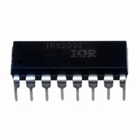
IRS2092PBF International Rectifier, IRS2092PBF Datasheet - Page 4

IRS2092PBF
Manufacturer Part Number
IRS2092PBF
Description
IC AMP AUDIO 500W MONO D 16DIP
Manufacturer
International Rectifier
Type
Class Dr
Datasheet
1.IRS2092PBF.pdf
(9 pages)
Specifications of IRS2092PBF
Output Type
1-Channel (Mono)
Voltage - Supply
10 V ~ 18 V
Features
Depop, PWM, Short-Circuit Protection
Mounting Type
Through Hole
Package / Case
16-DIP (0.300", 7.62mm)
Amplifier Type
Audio
Bandwidth
9 MHz
Common Mode Rejection Ratio
60
Current, Input Bias
40 nA
Current, Output
1 A
Current, Supply
3 mA (Low Side), 1 mA (High Side)
Impedance, Thermal
75 °C/W
Number Of Amplifiers
Single
Open Loop Gain
60
Package Type
PDIP-16
Power Dissipation
1.6 W
Propagation Delay
360 ns (Turn-On), 335 ns (Turn-Off)
Slew Rate
±5
Temperature, Operating, Range
-40 to +125 °C
Time, Fall
15 ns
Time, Rise
20 ns
Voltage, Input Offset
15 mV
Voltage, Noise
250 mVrms
Voltage, Supply
10 to 18 V
Amplifier Class
D
No. Of Channels
1
Output Power
500W
Supply Voltage Range
10V To 18V
Load Impedance
4ohm
Operating Temperature Range
-40°C To +125°C
Amplifier Case Style
DIP
Rohs Compliant
Yes
Channels
1
Package
16-pin DIP
Circuit
Half-Bridge Driver
Supply Voltage
200
Output Source Current Min (ma)
1000
Output Sink Current Min (ma)
1200
Vcc Range (v)
10-20V with UVLO
Pbf
Yes
For Use With
IRAUDAMP7S - BOARD REF DESIGN 2CH AUDIO AMPIRAUDAMP7D - KIT REF DESIGN AUD AMP D IRS2092IRAUDAMP5 - BOARD DEMO IRS2092S/IRF6645
Lead Free Status / RoHS Status
Lead free / RoHS Compliant
Max Output Power X Channels @ Load
-
Lead Free Status / Rohs Status
RoHS Compliant part
Available stocks
Company
Part Number
Manufacturer
Quantity
Price
Company:
Part Number:
IRS2092PBF
Manufacturer:
LT
Quantity:
1 001
Recommended Operating Conditions
Note 1: Logic operational for Vs equal to –5 V to +200 V. Logic state held for Vs equal to –5 V to –V
Note 2: Nominal voltage for V
Note 3: GND input voltage is limited by I
Note 4: V
Note 5: Output logic status may not respond correctly if input pulse width is smaller than the minimum pulse width.
For proper operation, the device should be used within the recommended conditions below. The Vs and COM offset ratings
are tested with supplies biased at V
referenced to COM; all currents are defined positive into any lead.
Symbol
dVss/dt
V
V
C
V
V
I
V
I
I
V
V
V
V
V
V
OREF
OCSET
f
COMP
COMP
I
V
V
AAZ
SSZ
T
GND
PW
SW
CSD
CSH
HO
CC
SS
LO
IN-
DT
A
B
S
16.7 kΩ.
SS
ramps up from 0 V to 200 V.
High side floating supply absolute voltage
High side floating supply offset voltage
Floating input positive supply zener clamp current
Floating input negative supply zener clamp current
Floating input supply absolute voltage
High side floating output voltage
Low side fixed supply voltage
Low side output voltage
GND pin input voltage
Inverting input voltage
CSD pin input voltage
COMP pin input voltage
COMP pin phase compensation capacitor to GND
DT pin input voltage
Reference output current to COM
OCSET pin input voltage
CSH pin input voltage
Allowable Vss voltage slew rate upon power-up
Input pulse width
Switching Frequency
Ambient Temperature
REF
is 5.1 V. I
AA
-V
Definition
AAZ
SS
=10 V, V
OREF
and I
of 0.3 – 0.8 mA dictates total external resistor value on VREF to be 6.3 kΩ to
SSZ
CC
(Note 2)
.
=12 V and V
7
B
(Note4)
-V
S
=12 V. All voltage parameters are absolute voltages
V
10
V
SS
(Note 1)
V
GND
Min.
(Note 5)
S
V
V
(Note 3)
0.3
0.5
-40
Vs
Vs
10
1
1
0
0
1
0
+10
-
-
SS
SS
-0.5
V
© 2007 International Rectifier
V
AA
V
GND
BS
Max.
S
200
200
V
V
800
125
(Note 3)
V
V
0.8
11
11
V
18
V
50
.
5
+18
-
-
CC
AA
AA
CC
B
B
+0.5
IRS2092
Units
V/ms
kHz
mA
mA
nF
ns
°C
V
V
V
V


