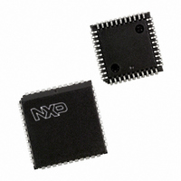
SCC2681TC1A44,529 NXP Semiconductors, SCC2681TC1A44,529 Datasheet - Page 4

SCC2681TC1A44,529
Manufacturer Part Number
SCC2681TC1A44,529
Description
IC DUART SOT187-2
Manufacturer
NXP Semiconductors
Type
Dual asynchronous receiver/transmitter (DUART)r
Datasheet
1.SCC2681TC1A44518.pdf
(15 pages)
Specifications of SCC2681TC1A44,529
Number Of Channels
2, DUART
Package / Case
44-LCC (J-Lead)
Features
False-start Bit Detection
Fifo's
3Bit
Voltage - Supply
4.5 V ~ 5.5 V
With Parallel Port
Yes
With Auto Flow Control
Yes
With False Start Bit Detection
Yes
With Cmos
Yes
Mounting Type
Surface Mount
Data Rate
0.1152 MBd
Supply Voltage (max)
5.5 V
Supply Voltage (min)
4.5 V
Supply Current
10 mA
Maximum Operating Temperature
+ 70 C
Minimum Operating Temperature
0 C
Mounting Style
SMD/SMT
Operating Supply Voltage
5 V
Lead Free Status / RoHS Status
Lead free / RoHS Compliant
Lead Free Status / RoHS Status
Lead free / RoHS Compliant, Lead free / RoHS Compliant
Other names
935274519529
SCC2681TC1A44-S
SCC2681TC1A44-S
SCC2681TC1A44-S
SCC2681TC1A44-S
Philips Semiconductors
PIN CONFIGURATION
PIN DESCRIPTION
2004 Apr 06
MNEMONIC
Dual asynchronous receiver/transmitter (DUART)
RESET
X1/CLK
D0–D7
A0–A3
INTRN
RxDA
RxDB
WRN
RDN
CEN
X2
21, 25, 20,
26, 19, 27,
2, 4, 6, 7
18, 28
PIN
39
10
38
24
36
37
35
11
9
TYPE
I/O
O
I
I
I
I
I
I
I
I
I
Data Bus: Bidirectional three-state data bus used to transfer commands, data and status between the
DUART and the CPU. D0 is the least significant bit.
Chip Enable: Active LOW input signal. When LOW, data transfers between the CPU and the DUART
are enabled on D0–D7 as controlled by the WRN, RDN, and A0–A3 inputs. When CEN is HIGH, the
DUART places the D0–D7 lines in the three-state condition.
Write Strobe: When LOW and CEN is also LOW, the contents of the data bus is loaded into the
addressed register. The transfer occurs on the rising edge of the signal.
Read Strobe: When low and CEN is also LOW, causes the contents of the addressed register to be
presented on the data bus. The read cycle begins on the falling edge of RDN.
Address Inputs: Select the DUART internal registers and ports for read/write operations.
Reset: A HIGH level clears internal registers (SRA, SRB, IMR, ISR, OPR, OPCR), puts OP0–OP7 in the
HIGH state, stops the counter/timer, and puts channels A and B in the inactive state, with the TxDA and
TxDB outputs in the mark (HIGH) state. Clears Test modes, sets MR pointer to MR1.
Interrupt Request: Active-LOW, open-drain output which signals the CPU that one or more of the eight
maskable interrupting conditions are true.
Crystal 1: Crystal connection or an external clock input. A crystal of a clock the appropriate frequency
(nominally 3.6864 MHz) must be supplied at all times. For crystal connections see Figure 7, Clock
Timing.
Crystal 2: Crystal connection. See Figure 7. If a crystal is not used it is best to keep this pin not
connected.
It must not be grounded.
Channel A Receiver Serial Data Input: The least significant bit is received first. ‘Mark’ is HIGH, ‘space’
is LOW.
Channel B Receiver Serial Data Input: The least significant bit is received first. ‘Mark’ is HIGH, ‘space’
is LOW.
VCC
IP6
IP5
n.c.
IP2
IP4
IP3
IP1
A1
A0
A2
40
41
42
43
44
1
2
3
4
5
6
Figure 2. Pin configuration
SCC2681TC1A44
4
NAME AND FUNCTION
28
27
26
25
24
23
22
21
20
19
18
SD00737
D0
D2
D4
D6
INTRN
n.c.
GND
D7
D5
D3
D1
SCC2681T
Product data


