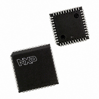
SCC2681TC1A44,518 NXP Semiconductors, SCC2681TC1A44,518 Datasheet - Page 7

SCC2681TC1A44,518
Manufacturer Part Number
SCC2681TC1A44,518
Description
IC DUART SOT187-2
Manufacturer
NXP Semiconductors
Datasheet
1.SCC2681TC1A44518.pdf
(15 pages)
Specifications of SCC2681TC1A44,518
Features
False-start Bit Detection
Number Of Channels
2, DUART
Fifo's
3Bit
Voltage - Supply
4.5 V ~ 5.5 V
With Parallel Port
Yes
With Auto Flow Control
Yes
With False Start Bit Detection
Yes
With Cmos
Yes
Mounting Type
Surface Mount
Package / Case
44-LCC (J-Lead)
Lead Free Status / RoHS Status
Lead free / RoHS Compliant
Other names
935274519518
SCC2681TC1A44-T
SCC2681TC1A44-T
SCC2681TC1A44-T
SCC2681TC1A44-T
1. Parameters are valid over specified temperature range.
2. All voltage measurements are referenced to ground (GND). For testing, all inputs swing between 0.4 V and 2.4 V with a transition time of
3. Typical values are at +25 C, typical supply voltages, and typical processing parameters.
4. Test conditions for outputs: C
5. All outputs are disconnected. Inputs are switching between CMOS levels of V
Philips Semiconductors
DC ELECTRICAL CHARACTERISTICS
T
NOTES:
2004 Apr 06
amb
SYMBOL
SYMBOL
V
V
V
V
V
V
I
I
I
I
I
I
I
I
I
I
I
I
I
I
IX1
ILX1
IHX1
OHX2
OHX2S
OLX2
OLX2S
I
OZH
OZL
ODL
ODH
CC
CC
Dual asynchronous receiver/transmitter (DUART)
IL
IH
IH
IH
OL
OH
5 ns maximum. For X1/CLK this swing is between 0.4 V and 4.4 V. All time measurements are referenced at input voltages of 0.8 V and
2.0 V and output voltages of 0.8 V and 2.0 V, as appropriate.
= 0 C to +70 C; V
LOW-level input voltage
HIGH-level input voltage (except X1/CLK)
HIGH-level input voltage (except X1/CLK)
HIGH-level input voltage (X1/CLK)
LOW-level output voltage
HIGH-level output voltage (except open-drain outputs)
X1/CLK input current
X1/CLK input LOW current – operating
X1/CLK input HIGH current – operating
X2 output HIGH current – operating
X2 output HIGH short circuit current – operating
X2 output LOW current – operating
X2 output LOW short circuit current – operating
Input leakage current:
Output off current HIGH, 3-state data bus
Output off current LOW, 3-state data bus
Open-drain output LOW current in off-state
Open-drain output HIGH current in off-state
Power supply current
All except input port pins
Input port pins
Operating mode
CC
= +5.0 V
L
= 150 pF, except interrupt outputs. Test conditions for interrupt outputs: C
5
PARAMETER
PARAMETER
10%
1, 2, 3
4
7
CC
V
V
TEST CONDITIONS
TEST CONDITIONS
V
OUT
V
OUT
CMOS input levels
– 0.2 V and V
OUT
V
V
V
OUT
I
IN
IN
IN
OH
I
T
OL
T
= V
amb
V
= 0 V; X1 = V
V
V
amb
V
V
V
= 0 V to V
= 0 V to V
= 0 V to V
= V
IN
= 0 V; X1 = 0
IN
IN
IN
IN
IN
= –400 A
= 2.4 mA
CC
= V
= V
= V
< 0 C
= 0 V
= 0 V
= 0 V
CC
; X1 = V
0 C
; X1 = 0
CC
CC
CC
SS
CC
CC
CC
+ 0.2 V.
CC
CC
V
L
0.8 V
CC
= 50 pF, R
Min
–10
–75
–10
–75
–10
–20
–10
–10
2.0
2.5
–
–
0
0
1
–
–
–
– 0.5
CC
LIMITS
L
Typ
= 2.7 k to V
SCC2681T
–
–
–
–
–
–
–
–
–
–
–
–
–
–
–
–
–
–
–
–
Max
+10
+75
+10
+10
0.8
0.4
75
–1
10
10
10
10
–
–
–
–
0
0
–
–
Product data
CC
UNIT
UNIT
.
mA
mA
mA
V
V
V
V
V
V
A
A
A
A
A
A
A
A
A
A
A


