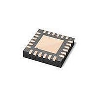
MAX3107ETG+ Maxim Integrated Products, MAX3107ETG+ Datasheet - Page 45

MAX3107ETG+
Manufacturer Part Number
MAX3107ETG+
Description
IC UART SPI/I2C 128 FIFO 24TQFN
Manufacturer
Maxim Integrated Products
Datasheet
1.MAX3107EAG.pdf
(52 pages)
Specifications of MAX3107ETG+
Features
Internal Oscillators
Number Of Channels
4, QUART
Fifo's
128 Byte
Protocol
RS232, RS485
Voltage - Supply
2.35 V ~ 3.6 V
With Auto Flow Control
Yes
With Irda Encoder/decoder
Yes
With False Start Bit Detection
Yes
Mounting Type
Surface Mount
Package / Case
24-TQFN Exposed Pad
Data Rate
24 Mbps
Supply Voltage (max)
3.3 V
Supply Voltage (min)
2.35 V
Supply Current
0.64 mA
Maximum Operating Temperature
+ 85 C
Minimum Operating Temperature
- 40 C
Mounting Style
SMD/SMT
No. Of Channels
1
Uart Features
128-Word Transmit / Receive FIFO, Half-Duplex Echo Suppression, Shutdown And Autosleep Modes
Supply Voltage Range
2.35V To 3.6V
Rohs Compliant
Yes
Lead Free Status / RoHS Status
Lead free / RoHS Compliant
When writing to the MAX3107 using I
sends a START condition (S) followed by the MAX3107
I
the register address of the register that is to be pro-
grammed. The master then ends communication by
issuing a STOP condition (P) to relinquish control of the
bus, or a repeated START condition (Sr) to communicate
to another I
The MAX3107 includes a 7-bit slave address. The first 5
bits (MSBs) of the slave address are factory-programmed
and always 01011. These slave addresses are unique
device IDs. Connect A1, A0 to ground or V
I
the 7 MSBs followed by the read/write bit. Set the read/
write bit to 1 to configure the MAX3107 to read mode. Set
the read/write bit to 0 to configure the MAX3107 to write
Figure 17. I
Table 5. I
2
2
C slave address (Table 5). The address is defined as
C address. After the address, the master sends
DIN/A1
0
0
1
1
START, STOP, and Repeated START Conditions
2
C START, STOP, and Repeated START Conditions
2
2
C slave. See Figure 17.
CS/A0
C Address Map
0
1
0
1
SDA
SCL
______________________________________________________________________________________
WRITE
READ/
W
W
W
W
R
R
R
R
SPI/I
S
I
2
C ADDRESS
2
Slave Address
C, the master
0x5C
0x5D
0x5A
0x5B
0x5E
2
0x58
0x59
0x5F
L
C UART with 128-Word FIFOs
to set the
mode. The address is the first byte of information sent to
the MAX3107 after the START condition.
One data bit is transferred during each SCL clock cycle.
The data on SDA must remain stable during the high
period of the SCL clock pulse. Changes in SDA while
SCL is high and stable are considered control signals
(see the START, STOP, and Repeated START Conditions
section). Both SDA and SCL remain high when the bus
is not active.
With this operation the master sends an address and 1
or 2 data bytes to the slave device (Figure 18). The write
byte procedure is as follows:
1) The master sends a START condition.
2) The master sends the 7-bit slave ID plus a write bit (low).
3) The addressed slave asserts an ACK on the data line.
4) The master sends the 8-bit register address.
5) The active slave asserts an ACK on the data line only
6) The master sends the 8-bit data byte.
7) The slave asserts an ACK on the data line.
8) The master generates a STOP condition.
With this operation the master sends an address and
multiple data bytes to the slave device (Figure 19). The
burst write procedure is as follows:
1) The master sends a START condition.
and Internal Oscillator
Sr
if the address is valid (NACK if not).
P
Single-Byte Write
Bit Transfer
Burst Write
45


