PC16550DN/NOPB National Semiconductor, PC16550DN/NOPB Datasheet - Page 16
PC16550DN/NOPB
Manufacturer Part Number
PC16550DN/NOPB
Description
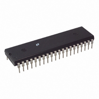
IC UART WITH FIFO 40-DIP
Manufacturer
National Semiconductor
Datasheet
1.PC16550DVNOPB.pdf
(22 pages)
Specifications of PC16550DN/NOPB
Features
Modem Control Function
Number Of Channels
1, UART
Fifo's
16 Byte
Voltage - Supply
4.5 V ~ 5.5 V
With False Start Bit Detection
Yes
With Modem Control
Yes
Mounting Type
Through Hole
Package / Case
40-DIP (0.600", 15.24mm)
Supply Voltage (max)
5.5 V
Supply Voltage (min)
4.5 V
Msl
MSL 1 - Unlimited
Data Rate Max
128Kbps
Ic Function
UART IC
Interface Type
Serial
No. Of Transceivers
1
Peak Reflow Compatible (260 C)
Yes
Supply Current
15mA
Rohs Compliant
Yes
Lead Free Status / RoHS Status
Lead free / RoHS Compliant
Other names
*PC16550DN
*PC16550DN/NOPB
PC16550DN
*PC16550DN/NOPB
PC16550DN
Available stocks
Company
Part Number
Manufacturer
Quantity
Price
Company:

Part Number:
PC16550DN/NOPB
Manufacturer:
NSC
Quantity:
1 011
Company:
Part Number:
PC16550DN/NOPB
Manufacturer:
National
Quantity:
695
Part Number:
PC16550DN/NOPB
Manufacturer:
TI/德州仪器
Quantity:
20 000


8 0 Registers
Bit 7 This bit is the Divisor Latch Access Bit (DLAB) It must
be set high (logic 1) to access the Divisor Latches of the
Baud Generator during a Read or Write operation It must
be set low (logic 0) to access the Receiver Buffer the
Transmitter Holding Register or the Interrupt Enable Regis-
ter
8 2 TYPICAL CLOCK CIRCUITS
Note These R and C values are approximate and may vary 2x depending
8 3 PROGRAMMABLE BAUD GENERATOR
The UART contains a programmable Baud Generator that is
capable of taking any clock input from DC to 24 MHz and
dividing it by any divisor from 2 to 2
quency of the Baud Generator is 16
store the divisor in a 16-bit binary format These Divisor
Latches must be loaded during initialization to ensure prop-
er operation of the Baud Generator Upon loading either of
the Divisor Latches a 16-bit Baud counter is immediately
loaded
Table III provides decimal divisors to use with crystal fre-
quencies of 1 8432 MHz 3 072 MHz and 18 432 MHz re-
spectively For baud rates of 38400 and below the error
obtained is minimal The accuracy of the desired baud rate
is dependent on the crystal frequency chosen Using a divi-
sor of zero is not recommended
e
CRYSTAL
(frequency input)
3 1 MHz
1 8 MHz
on the crystal characteristics All crystal circuits should be designed
specifically for the system
Typical Crystal Oscillator Network (Note)
1 M
1 M
R
P
d
(baud rate
(Continued)
1 5k
1 5k
R
X2
c
10-30 pF
10-30 pF
c
16) Two 8-bit latches
16
C
b
the Baud divisor
1
1 The output fre-
TL C 8652–19
TL C 8652–20
40-60 pF
40-60 pF
C
2
16
8 4 LINE STATUS REGISTER
This register provides status information to the CPU con-
cerning the data transfer Table II shows the contents of the
Line Status Register Details on each bit follow
Bit 0 This bit is the receiver Data Ready (DR) indicator Bit
0 is set to a logic 1 whenever a complete incoming charac-
ter has been received and transferred into the Receiver
Buffer Register or the FIFO Bit 0 is reset to a logic 0 by
reading all of the data in the Receiver Buffer Register or the
FIFO
Bit 1 This bit is the Overrun Error (OE) indicator Bit 1 indi-
cates that data in the Receiver Buffer Register was not read
by the CPU before the next character was transferred into
the Receiver Buffer Register thereby destroying the previ-
ous character The OE indicator is set to a logic 1 upon
detection of an overrun condition and reset whenever the
CPU reads the contents of the Line Status Register If the
FIFO mode data continues to fill the FIFO beyond the trig-
ger level an overrun error will occur only after the FIFO is
full and the next character has been completely received in
the shift register OE is indicated to the CPU as soon as it
happens The character in the shift register is overwritten
but it is not transferred to the FIFO
Bit 2 This bit is the Parity Error (PE) indicator Bit 2 indi-
cates that the received data character does not have the
correct even or odd parity as selected by the even-parity-
select bit The PE bit is set to a logic 1 upon detection of a
parity error and is reset to a logic 0 whenever the CPU reads
the contents of the Line Status Register In the FIFO mode
this error is associated with the particular character in the
FIFO it applies to This error is revealed to the CPU when its
associated character is at the top of the FIFO
Bit 3 This bit is the Framing Error (FE) indicator Bit 3 indi-
cates that the received character did not have a valid Stop
bit Bit 3 is set to a logic 1 whenever the Stop bit following
the last data bit or parity bit is detected as a logic 0 bit
(Spacing level) The FE indicator is reset whenever the CPU
reads the contents of the Line Status Register In the FIFO
mode this error is associated with the particular character in
the FIFO it applies to This error is revealed to the CPU
when its associated character is at the top of the FIFO The
UART will try to resynchronize after a framing error To do
this it assumes that the framing error was due to the next
start bit so it samples this ‘‘start’’ bit twice and then takes in
the ‘‘data’’
Bit 4 This bit is the Break Interrupt (BI) indicator Bit 4 is set
to a logic 1 whenever the received data input is held in the
Spacing (logic 0) state for longer than a full word transmis-
sion time (that is the total time of Start bit
Parity
CPU reads the contents of the Line Status Register In the
FIFO mode this error is associated with the particular char-
acter in the FIFO it applies to This error is revealed to the
CPU when its associated character is at the top of the FIFO
When break occurs only one zero character is loaded into
the FIFO The next character transfer is enabled after SIN
goes to the marking state and receives the next valid start
bit
Note Bits 1 through 4 are the error conditions that produce a Receiver Line
Status interrupt whenever any of the corresponding conditions are
detected and the interrupt is enabled
a
Stop bits) The BI indicator is reset whenever the
a
data bits
a
Related parts for PC16550DN/NOPB
Image
Part Number
Description
Manufacturer
Datasheet
Request
R

Part Number:
Description:
UART IC
Manufacturer:
National Semiconductor
Datasheet:

Part Number:
Description:
National Semiconductor [8-Bit D/A Converter]
Manufacturer:
National Semiconductor
Datasheet:
Part Number:
Description:
National Semiconductor [Media Coprocessor]
Manufacturer:
National Semiconductor
Datasheet:
Part Number:
Description:
Digitally Controlled Tone and Volume Circuit with Stereo Audio Power Amplifier, Microphone Preamp Stage and National 3D Sound
Manufacturer:
National Semiconductor
Datasheet:
Part Number:
Description:
Digitally Controlled Tone and Volume Circuit with Stereo Audio Power Amplifier, Microphone Preamp Stage and National 3D Sound
Manufacturer:
National Semiconductor
Datasheet:
Part Number:
Description:
AC97 Rev 2 Codec with Sample Rate Conversion and National 3D Sound
Manufacturer:
National Semiconductor
Part Number:
Description:
Manufacturer:
National Semiconductor
Datasheet:
Part Number:
Description:
Manufacturer:
National Semiconductor
Datasheet:
Part Number:
Description:
General Purpose, Low Voltage, Low Power, Rail-to-Rail Output Operational Amplifiers
Manufacturer:
National Semiconductor
Datasheet:
Part Number:
Description:
8-bit 20 MSPS flash A/D converter.
Manufacturer:
National Semiconductor
Datasheet:
Part Number:
Description:
Low Noise Quad Operational Amplifier
Manufacturer:
National Semiconductor
Datasheet:
Part Number:
Description:
Quad Differential Line Receivers
Manufacturer:
National Semiconductor
Datasheet:
Part Number:
Description:
Quad High Speed Trapezoidal? Bus Transceiver
Manufacturer:
National Semiconductor
Datasheet:
Part Number:
Description:
Dual Line Receiver
Manufacturer:
National Semiconductor
Datasheet: