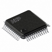
SC16C652BIB48,128 NXP Semiconductors, SC16C652BIB48,128 Datasheet - Page 8

SC16C652BIB48,128
Manufacturer Part Number
SC16C652BIB48,128
Description
IC ENCODER/DECODER IRDA 48LQFP
Manufacturer
NXP Semiconductors
Datasheet
1.SC16C652BIB48128.pdf
(43 pages)
Specifications of SC16C652BIB48,128
Features
2 Channels
Number Of Channels
2, DUART
Fifo's
32 Byte
Voltage - Supply
2.5V, 3.3V, 5V
With Auto Flow Control
Yes
With Irda Encoder/decoder
Yes
With False Start Bit Detection
Yes
With Modem Control
Yes
With Cmos
Yes
Mounting Type
Surface Mount
Package / Case
48-LQFP
Lead Free Status / RoHS Status
Lead free / RoHS Compliant
Other names
935274409128
SC16C652BIB48-F
SC16C652BIB48-F
SC16C652BIB48-F
SC16C652BIB48-F
Available stocks
Company
Part Number
Manufacturer
Quantity
Price
Company:
Part Number:
SC16C652BIB48,128
Manufacturer:
NXP Semiconductors
Quantity:
10 000
Philips Semiconductors
SC16C652B_4
Product data sheet
6.1 UART A-B functions
6.2 Internal registers
The UART provides the user with the capability to bi-directionally transfer information
between an external CPU, the SC16C652B package, and an external serial device. A
logic 0 on chip select pins CSA and/or CSB allows the user to configure, send data,
and/or receive data via UART channels A-B. Individual channel select functions are shown
in
Table 3:
The SC16C652B provides two sets of internal registers (A and B) consisting of
17 registers each for monitoring and controlling the functions of each channel of the
UART. These registers are shown in
registers (THR/RHR), interrupt status and control registers (IER/ISR), a FIFO Control
Register (FCR), line status and control registers (LCR/LSR), modem status and control
registers (MCR/MSR), programmable data rate (clock) control registers (DLL/DLM), and a
user accessible Scratchpad Register (SPR).
Table 4:
[1]
[2]
[3]
Chip Select
CSA-CSB = 1
CSA = 0
CSB = 0
A2
General register set (THR/RHR, IER/ISR, MCR/MSR, FCR, LSR, SPR)
0
0
0
0
1
1
1
1
Baud rate register set (DLL/DLM)
0
0
Enhanced register set (EFR, Xon1/Xon2, Xoff1/Xoff2)
0
1
1
1
1
Table
These registers are accessible only when LCR[7] is a logic 0.
These registers are accessible only when LCR[7] is a logic 1.
Enhanced Feature Register, Xon1/Xon2 and Xoff1/Xoff2 are accessible only when the LCR is set to ‘BFh’.
A1
0
0
1
1
0
0
1
1
0
0
1
0
0
1
1
3.
Serial port selection
Internal registers decoding
A0
0
1
0
1
0
1
0
1
0
1
0
0
1
0
1
Rev. 04 — 1 September 2005
Function
none
UART channel A
UART channel B
Read mode
Receive Holding Register
Interrupt Enable Register
Interrupt Status Register
Line Control Register
Modem Control Register
Line Status Register
Modem Status Register
Scratchpad Register
LSB of Divisor Latch
MSB of Divisor Latch
Enhanced Feature Register
Xon1 word
Xon2 word
Xoff1 word
Xoff2 word
Dual UART with 32-byte FIFOs and IrDA encoder/decoder
[2]
Table
4. The UART registers function as data holding
[3]
Write mode
Transmit Holding Register
Interrupt Enable Register
FIFO Control Register
Line Control Register
Modem Control Register
n/a
n/a
Scratchpad Register
LSB of Divisor Latch
MSB of Divisor Latch
Enhanced Feature Register
Xon1 word
Xon2 word
Xoff1 word
Xoff2 word
© Koninklijke Philips Electronics N.V. 2005. All rights reserved.
SC16C652B
[1]
8 of 43


