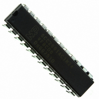
SCC2691AC1N24,602 NXP Semiconductors, SCC2691AC1N24,602 Datasheet - Page 20

SCC2691AC1N24,602
Manufacturer Part Number
SCC2691AC1N24,602
Description
IC UART SINGLE 24-DIP
Manufacturer
NXP Semiconductors
Type
Single Channel UARTr
Datasheet
1.SCC2691AC1A28623.pdf
(25 pages)
Specifications of SCC2691AC1N24,602
Number Of Channels
1, UART
Package / Case
24-DIP (0.300", 7.62mm)
Features
False-start Bit Detection
Fifo's
3Bit
Voltage - Supply
5V
With Auto Flow Control
Yes
With False Start Bit Detection
Yes
With Cmos
Yes
Mounting Type
Through Hole
Data Rate
0.1152 MBd
Supply Voltage (max)
5.5 V
Supply Voltage (min)
4.5 V
Supply Current
2 mA
Maximum Operating Temperature
+ 70 C
Minimum Operating Temperature
0 C
Mounting Style
SMD/SMT
Operating Supply Voltage
5 V
Lead Free Status / RoHS Status
Lead free / RoHS Compliant
Lead Free Status / RoHS Status
Lead free / RoHS Compliant, Lead free / RoHS Compliant
Other names
568-1213-5
933811540602
SCC2691AC1N24
933811540602
SCC2691AC1N24
Philips Semiconductors
Table 6. Baud Rates Extended
NOTE:
Each read on address H‘2’ will toggle the baud rate test mode. When in the BRG test mode, the baud rates change as shown to the left. This
change affects all receivers and transmitters on the DUART. See “Extended baud rates for SCN2681, SCN68681, SCC2691, SCC2692,
SCC68681 and SCC2698B” in application notes elsewhere in this publication.
The test mode at address H‘A’ changes all transmitters and receivers to the 1x mode and connects the output ports to some internal nodes.
2006 Aug 04
Universal asynchronous receiver/transmitter (UART)
Receiver Reset in the Normal Mode (Receiver Enabled)
Reset can be accomplished easily by issuing a receiver software or hardware reset followed by a receiver enable. All receiver data,
status and programming will be preserved and available before reset. The reset will NOT affect the programming.
Receiver Reset in the Wake-Up Mode (MR1[4:3] = 11)
Reset can also be accomplished easily by first exiting the wake-up mode (MR1[4:3] = 00 or 01 or 10), then issuing a receiver software or
hardware reset followed by a wake-up re-entry (MR1[4:3] = 11). All receiver data, status and programming will be preserved and
available before reset. The reset will NOT affect other programming.
The reason for this is the receiver is partially enabled when the parity bits are at ‘11’. Thus the receiver disable and reset is bypassed by
the partial enabling of the receiver.
CSR[7:4]
0000
0001
0010
0011
0100
0101
0110
0111
1000
1001
1010
1011
1100
1101
1110
1111
ACR[7] = 0
I/O2 – 16X
I/O2 – 1X
38.4K
134.5
1,200
1,050
2,400
4,800
7,200
9,600
Timer
110
200
300
600
50
Normal BRG
ACR[7] = 1
I/O2 – 16X
I/O2 – 1X
19.2K
134.5
1,200
2,000
2,400
4,800
1,800
9,600
Timer
150
300
600
110
75
20
ACR[7] = 0
I/O2 – 16X
I/O2 – 1X
115.2K
19.2K
28.8K
57.6K
57.6K
57.6K
38.4K
4,800
1,076
1,050
4,800
9,600
Timer
880
BRG Test
ACR[7] = 1
I/O2 – 16X
I/O2 – 1X
SCC2691
115.2K
Product data sheet
14.4K
28.8K
57.6K
57.6K
14.4K
19.2K
7,200
1,076
2,000
4,800
9,600
Timer
880
SD00097


