SC16IS752IPW,112 NXP Semiconductors, SC16IS752IPW,112 Datasheet - Page 7
SC16IS752IPW,112
Manufacturer Part Number
SC16IS752IPW,112
Description
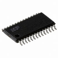
IC UART DUAL 12C/SPI 28TSSOP
Manufacturer
NXP Semiconductors
Type
IrDA or RS- 232 or RS- 485r
Datasheet
1.SC16IS752IBS151.pdf
(59 pages)
Specifications of SC16IS752IPW,112
Number Of Channels
2, DUART
Package / Case
28-TSSOP (0.173", 4.40mm Width)
Features
Low Current
Fifo's
64 Byte
Protocol
RS232, RS485
Voltage - Supply
2.5V, 3.3V
With Auto Flow Control
Yes
With Irda Encoder/decoder
Yes
With False Start Bit Detection
Yes
With Modem Control
Yes
Mounting Type
Surface Mount
Data Rate
5 Mbps
Supply Voltage (max)
3.6 V
Supply Voltage (min)
2.3 V
Supply Current
6 mA
Maximum Operating Temperature
+ 95 C
Minimum Operating Temperature
- 40 C
Mounting Style
SMD/SMT
Operating Supply Voltage
2.5 V or 3.3 V
Lead Free Status / RoHS Status
Lead free / RoHS Compliant
For Use With
568-4000 - DEMO BOARD SPI/I2C TO DUAL UART568-3510 - DEMO BOARD SPI/I2C TO UART
Lead Free Status / Rohs Status
Lead free / RoHS Compliant
Other names
568-4016-5
935279292112
SC16IS752IPW
SC16IS752IPW
935279292112
SC16IS752IPW
SC16IS752IPW


NXP Semiconductors
Table 2.
[1]
[2]
[3]
[4]
[5]
SC16IS752_SC16IS762_7
Product data sheet
Symbol
RESET
RTSA
RTSB
RXA
RXB
TXA
TXB
V
V
V
XTAL1
XTAL2
DD
SS
SS
Selectable with IOControl register bit 2.
Selectable with IOControl register bit 1.
See
HVQFN32 package die supply ground is connected to both V
ground for proper device operation. For enhanced thermal, electrical, and board level performance, the exposed pad needs to be
soldered to the board using a corresponding thermal pad on the board and for proper heat conduction through the board, thermal vias
need to be incorporated in the PCB in the thermal pad region.
XTAL2 should be left open when XTAL1 is driven by an external clock.
Section 7.4 “Hardware Reset, Power-On Reset (POR) and Software
Pin description
Pin
TSSOP28
5
1
17
4
24
3
23
8
22
-
6
7
…continued
HVQFN32
2
30
16
1
23
32
22
5, 13, 28
12, 21,
29
center
pad
3
4
[4]
[4]
Type Description
I
O
O
I
I
O
O
-
-
-
I
O
Dual UART with I
Hardware reset (active LOW)
UART request to send (active LOW), channel A. A logic 0 on the RTSA
pin indicates the transmitter has data ready and waiting to send. Writing
a logic 1 in the Modem Control Register MCR[1] will set this pin to a
logic 0, indicating data is available. After a reset this pin is set to a logic 1.
This pin only affects the transmit and receive operations when Auto-RTS
function is enabled via the Enhanced Features Register (EFR[6]) for
hardware flow control operation.
UART request to send (active LOW), channel B. A logic 0 on the RTSB
pin indicates the transmitter has data ready and waiting to send. Writing
a logic 1 in the Modem Control Register MCR[1] will set this pin to a
logic 0, indicating data is available. After a reset this pin is set to a logic 1.
This pin only affects the transmit and receive operations when Auto-RTS
function is enabled via the Enhanced Features Register (EFR[6]) for
hardware flow control operation.
Channel A receiver input. During the local Loopback mode, the RXA
input pin is disabled and TXA data is connected to the UART RXA input
internally.
Channel B receiver input. During the local Loopback mode, the RXB
input pin is disabled and TXB data is connected to the UART RXB input
internally.
Channel A transmitter output. During the local Loopback mode, the TXA
output pin is disabled and TXA data is internally connected to the UART
RXA input.
Channel B transmitter output. During the local Loopback mode, the TXB
output pin is disabled and TXB data is internally connected to the UART
RXB input.
Power supply
Ground
The center pad on the back side of the HVQFN32 package is metallic
and should be connected to ground on the printed-circuit board.
Crystal input or external clock input. A crystal can be connected between
XTAL1 and XTAL2 to form an internal oscillator circuit (see
Alternatively, an external clock can be connected to this pin.
Crystal output. (See also XTAL1.) XTAL2 is used as a crystal oscillator
output
Rev. 07 — 19 May 2008
[5]
SS
.
pins and exposed center pad. V
Reset”.
2
SC16IS752/SC16IS762
C-bus/SPI interface, 64-byte FIFOs, IrDA SIR
[3]
SS
pins must be connected to supply
© NXP B.V. 2008. All rights reserved.
Figure
11).
7 of 59
Related parts for SC16IS752IPW,112
Image
Part Number
Description
Manufacturer
Datasheet
Request
R

Part Number:
Description:
NXP Semiconductors designed the LPC2420/2460 microcontroller around a 16-bit/32-bitARM7TDMI-S CPU core with real-time debug interfaces that include both JTAG andembedded trace
Manufacturer:
NXP Semiconductors
Datasheet:

Part Number:
Description:
NXP Semiconductors designed the LPC2458 microcontroller around a 16-bit/32-bitARM7TDMI-S CPU core with real-time debug interfaces that include both JTAG andembedded trace
Manufacturer:
NXP Semiconductors
Datasheet:
Part Number:
Description:
NXP Semiconductors designed the LPC2468 microcontroller around a 16-bit/32-bitARM7TDMI-S CPU core with real-time debug interfaces that include both JTAG andembedded trace
Manufacturer:
NXP Semiconductors
Datasheet:
Part Number:
Description:
NXP Semiconductors designed the LPC2470 microcontroller, powered by theARM7TDMI-S core, to be a highly integrated microcontroller for a wide range ofapplications that require advanced communications and high quality graphic displays
Manufacturer:
NXP Semiconductors
Datasheet:
Part Number:
Description:
NXP Semiconductors designed the LPC2478 microcontroller, powered by theARM7TDMI-S core, to be a highly integrated microcontroller for a wide range ofapplications that require advanced communications and high quality graphic displays
Manufacturer:
NXP Semiconductors
Datasheet:
Part Number:
Description:
The Philips Semiconductors XA (eXtended Architecture) family of 16-bit single-chip microcontrollers is powerful enough to easily handle the requirements of high performance embedded applications, yet inexpensive enough to compete in the market for hi
Manufacturer:
NXP Semiconductors
Datasheet:
Part Number:
Description:
The XA-S3 device is a member of Philips Semiconductors? XA(eXtended Architecture) family of high performance 16-bitsingle-chip microcontrollers
Manufacturer:
NXP Semiconductors
Datasheet:

Part Number:
Description:
The NXP BlueStreak LH75401/LH75411 family consists of two low-cost 16/32-bit System-on-Chip (SoC) devices
Manufacturer:
NXP Semiconductors
Datasheet:
Part Number:
Description:
The NXP LPC3130/3131 combine an 180 MHz ARM926EJ-S CPU core, high-speed USB2
Manufacturer:
NXP Semiconductors
Datasheet:
Part Number:
Description:
The NXP LPC3141 combine a 270 MHz ARM926EJ-S CPU core, High-speed USB 2
Manufacturer:
NXP Semiconductors
Part Number:
Description:
The NXP LPC3143 combine a 270 MHz ARM926EJ-S CPU core, High-speed USB 2
Manufacturer:
NXP Semiconductors

Part Number:
Description:
The NXP LPC3152 combines an 180 MHz ARM926EJ-S CPU core, High-speed USB 2
Manufacturer:
NXP Semiconductors
Part Number:
Description:
The NXP LPC3154 combines an 180 MHz ARM926EJ-S CPU core, High-speed USB 2
Manufacturer:
NXP Semiconductors

Part Number:
Description:
Standard level N-channel enhancement mode Field-Effect Transistor (FET) in a plastic package using NXP High-Performance Automotive (HPA) TrenchMOS technology
Manufacturer:
NXP Semiconductors
Datasheet: