SC16C550BIA44,512 NXP Semiconductors, SC16C550BIA44,512 Datasheet - Page 8
SC16C550BIA44,512
Manufacturer Part Number
SC16C550BIA44,512
Description
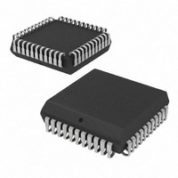
IC UART SINGLE W/FIFO 44-PLCC
Manufacturer
NXP Semiconductors
Datasheet
1.SC16C550BIA44518.pdf
(48 pages)
Specifications of SC16C550BIA44,512
Features
Programmable
Number Of Channels
1, UART
Fifo's
16 Byte
Voltage - Supply
2.5V, 3.3V, 5V
With Auto Flow Control
Yes
With False Start Bit Detection
Yes
With Modem Control
Yes
With Cmos
Yes
Mounting Type
Surface Mount
Package / Case
44-LCC (J-Lead)
Lead Free Status / RoHS Status
Lead free / RoHS Compliant
Other names
935274387512
SC16C550BIA44
SC16C550BIA44
SC16C550BIA44
SC16C550BIA44
Available stocks
Company
Part Number
Manufacturer
Quantity
Price
Company:

Part Number:
SC16C550BIA44,512
Manufacturer:
NXP Semiconductors
Quantity:
10 000


NXP Semiconductors
Table 2.
SC16C550B_5
Product data sheet
Symbol
RI
RTS
RXRDY
RX
TX
TXRDY
V
V
DD
SS
[2]
Pin description
Pin
PLCC44 LQFP48 DIP40 HVQFN32
43
36
32
11
13
27
44
22
41
32
29
7
8
23
42
18
…continued
39
32
29
10
11
24
40
20
27
21
-
6
7
-
28
9, 13
[1]
Rev. 05 — 1 October 2008
Type
I
O
O
I
O
O
power
power
Description
Ring indicator. RI is a modem status signal. Its condition
can be checked by reading bit 6 (RI) of the Modem Status
Register. Bit 2 ( RI) of the Modem Status Register
indicates that RI has changed from a LOW to a HIGH level
since the last read from the Modem Status Register. If the
modem status interrupt is enabled when this transition
occurs, an interrupt is generated.
Request to send. When active, RTS informs the modem
or data set that the UART is ready to receive data. RTS is
set to the active level by setting the RTS Modem Control
Register bit and is set to the inactive (HIGH) level either as
a result of a Master Reset or during loopback mode
operations or by clearing bit 1 (RTS) of the MCR. This pin
has no effect on the UART’s transmit or receive operation.
Receiver ready. Receiver Direct Memory Access (DMA)
signaling is available with RXRDY. When operating in the
FIFO mode, one of two types of DMA signaling can be
selected using the FIFO Control Register bit 3 (FCR[3]).
When operating in the 16C450 mode, only DMA mode 0 is
allowed. Mode 0 supports single-transfer DMA in which a
transfer is made between CPU bus cycles. Mode 1
supports multi-transfer DMA in which multiple transfers are
made continuously until the receiver FIFO has been
emptied. In DMA mode 0 (FCR[0] = 0 or FCR[0] = 1,
FCR[3] = 0), when there is at least one character in the
receiver FIFO or Receiver Holding Register, RXRDY is
active (LOW). When RXRDY has been active but there are
no characters in the FIFO or holding register, RXRDY goes
inactive (HIGH). In DMA mode 1 (FCR[0] = 1, FCR[3] = 1),
when the trigger level or the time-out has been reached,
RXRDY goes active (LOW); when it has been active but
there are no more characters in the FIFO or holding
register, it goes inactive (HIGH). This function does not
exist in the HVQFN32 package.
Serial data input. RX is serial data input from a connected
communications device.
Serial data output. TX is composite serial data output to a
connected communication device. TX is set to the marking
(HIGH) level as a result of Master Reset.
Transmitter ready. Transmitter DMA signaling is available
with TXRDY. When operating in the FIFO mode, one of
two types of DMA signaling can be selected using FCR[3].
When operating in the 16C450 mode, only DMA mode 0 is
allowed. Mode 0 supports single-transfer DMA in which a
transfer is made between CPU bus cycles. Mode 1
supports multi-transfer DMA in which multiple transfers are
made continuously until the transmit FIFO has been filled.
This function does not exist in the HVQFN32 package.
2.5 V, 3.3 V or 5 V supply voltage.
Ground voltage.
5 V, 3.3 V and 2.5 V UART with 16-byte FIFOs
SC16C550B
© NXP B.V. 2008. All rights reserved.
8 of 48
Related parts for SC16C550BIA44,512
Image
Part Number
Description
Manufacturer
Datasheet
Request
R

Part Number:
Description:
NXP Semiconductors designed the LPC2420/2460 microcontroller around a 16-bit/32-bitARM7TDMI-S CPU core with real-time debug interfaces that include both JTAG andembedded trace
Manufacturer:
NXP Semiconductors
Datasheet:

Part Number:
Description:
NXP Semiconductors designed the LPC2458 microcontroller around a 16-bit/32-bitARM7TDMI-S CPU core with real-time debug interfaces that include both JTAG andembedded trace
Manufacturer:
NXP Semiconductors
Datasheet:
Part Number:
Description:
NXP Semiconductors designed the LPC2468 microcontroller around a 16-bit/32-bitARM7TDMI-S CPU core with real-time debug interfaces that include both JTAG andembedded trace
Manufacturer:
NXP Semiconductors
Datasheet:
Part Number:
Description:
NXP Semiconductors designed the LPC2470 microcontroller, powered by theARM7TDMI-S core, to be a highly integrated microcontroller for a wide range ofapplications that require advanced communications and high quality graphic displays
Manufacturer:
NXP Semiconductors
Datasheet:
Part Number:
Description:
NXP Semiconductors designed the LPC2478 microcontroller, powered by theARM7TDMI-S core, to be a highly integrated microcontroller for a wide range ofapplications that require advanced communications and high quality graphic displays
Manufacturer:
NXP Semiconductors
Datasheet:
Part Number:
Description:
The Philips Semiconductors XA (eXtended Architecture) family of 16-bit single-chip microcontrollers is powerful enough to easily handle the requirements of high performance embedded applications, yet inexpensive enough to compete in the market for hi
Manufacturer:
NXP Semiconductors
Datasheet:
Part Number:
Description:
The XA-S3 device is a member of Philips Semiconductors? XA(eXtended Architecture) family of high performance 16-bitsingle-chip microcontrollers
Manufacturer:
NXP Semiconductors
Datasheet:

Part Number:
Description:
The NXP BlueStreak LH75401/LH75411 family consists of two low-cost 16/32-bit System-on-Chip (SoC) devices
Manufacturer:
NXP Semiconductors
Datasheet:
Part Number:
Description:
The NXP LPC3130/3131 combine an 180 MHz ARM926EJ-S CPU core, high-speed USB2
Manufacturer:
NXP Semiconductors
Datasheet:
Part Number:
Description:
The NXP LPC3141 combine a 270 MHz ARM926EJ-S CPU core, High-speed USB 2
Manufacturer:
NXP Semiconductors
Part Number:
Description:
The NXP LPC3143 combine a 270 MHz ARM926EJ-S CPU core, High-speed USB 2
Manufacturer:
NXP Semiconductors

Part Number:
Description:
The NXP LPC3152 combines an 180 MHz ARM926EJ-S CPU core, High-speed USB 2
Manufacturer:
NXP Semiconductors
Part Number:
Description:
The NXP LPC3154 combines an 180 MHz ARM926EJ-S CPU core, High-speed USB 2
Manufacturer:
NXP Semiconductors

Part Number:
Description:
Standard level N-channel enhancement mode Field-Effect Transistor (FET) in a plastic package using NXP High-Performance Automotive (HPA) TrenchMOS technology
Manufacturer:
NXP Semiconductors
Datasheet: