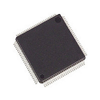
AD8113JST Analog Devices Inc, AD8113JST Datasheet

AD8113JST
Specifications of AD8113JST
Available stocks
Related parts for AD8113JST
AD8113JST Summary of contents
Page 1
FEATURES 16 16 High Speed Nonblocking Switch Array Serial or Parallel Programming of Switch Array Serial Data Out Allows Daisy Chaining Control of Multiple 16 16s to Create Larger Switch Arrays Output Disable Allows Connection of Multiple Devices without ...
Page 2
AD8113–SPECIFICATIONS Parameter DYNAMIC PERFORMANCE –3 dB Bandwidth Gain Flatness Propagation Delay Settling Time Slew Rate NOISE/DISTORTION PERFORMANCE Differential Gain Error Differential Phase Error Total Harmonic Distortion Crosstalk, All Hostile Off Isolation Input Voltage Noise DC PERFORMANCE Gain Error Gain Matching ...
Page 3
Parameter DYNAMIC PERFORMANCE Supply Voltage Range PSRR OPERATING TEMPERATURE RANGE Temperature Range θ JA Specifications subject to change without notice. TIMING CHARACTERISTICS (Serial) Parameter Serial Data Setup Time CLK Pulsewidth Serial Data Hold Time CLK Pulse Separation, Serial Mode CLK ...
Page 4
AD8113 TIMING CHARACTERISTICS (Parallel) Parameter Data Setup Time CLK Pulsewidth Data Hold Time CLK Pulse Separation CLK to UPDATE Delay UPDATE Pulsewidth Propagation Delay, UPDATE to Switch On or Off CLK, UPDATE Rise and Fall Times RESET Time Specifications subject ...
Page 5
... V potential differen- OUT tial. See output voltage swing specification for linear output range. Model AD8113JST AD8113-EVAL CAUTION ESD (electrostatic discharge) sensitive device. Electrostatic charges as high as 4000 V readily accumulate on the human body and test equipment and can discharge without detection. ...
Page 6
AD8113 CE UPDATE CLK DATA Data D4 PARALLEL D1 DATA ...
Page 7
Mnemonic Pin Numbers INxx 58, 60, 62, 64, 66, 68, 70, 72 10, 12, 14, 16, 18 DATA IN 96 CLK 97 DATA OUT 98 UPDATE 95 RESET 100 CE 99 SER/PAR 94 OUTyy 53, 51, 49, ...
Page 8
AD8113 PIN 1 DGND 2 IDENTIFIER 3 AGND IN08 4 AGND 5 IN09 6 AGND 7 IN10 8 AGND 9 IN11 10 AGND 11 IN12 12 AGND 13 IN13 14 AGND 15 IN14 16 AGND 17 IN15 ...
Page 9
FREQUENCY – MHz TPC 1. Small Signal Bandwidth 200 mV p-p OUT 0.3 0.2 0.1 0.0 –0.1 –0.2 –0.3 1 0.1 FREQUENCY – MHz TPC 2. Small Signal Gain Flatness, ...
Page 10
AD8113 0.3 0.2 0.1 0.0 –0.1 –0.2 –0.3 1 0.1 FREQUENCY – MHz TPC 7. Large Signal Gain Flatness p-p OUT –40 ALL HOSTILE –50 –60 –70 –80 –90 –100 1 0.1 FREQUENCY – MHz ...
Page 11
V = 12V 150 600 L 100 SERIES RESISTANCE – TPC 13. Cap Load vs. Series Resistance for Less than 30% Overshoot 10k 1k 100 10 1 ...
Page 12
AD8113 0 –10 –20 –30 –40 +PSRR –50 –PSRR –60 –70 –80 –90 0.01 0.1 FREQUENCY – MHz TPC 19. PSRR vs. Frequency, V 160 140 120 100 100 1k 10k FREQUENCY – Hz ...
Page 13
TPC 25. Large Signal Pulse Response 150 Ω 2V/DIV 100ns/DIV = ± TPC 26. Switching Time 1V/DIV OUTPUT 20mV/DIV 100ns/DIV TPC 27. Switching Transient REV. A 5V/DIV ...
Page 14
AD8113 THEORY OF OPERATION The AD8113 is a gain-of-two crosspoint array with 16 outputs, each of which can be connected to any one of 16 inputs. Organized by output row, 16 switchable transconductance stages are connected to each output buffer ...
Page 15
CALCULATION OF POWER DISSIPATION 4.0 3.5 3.0 2.5 2 AMBIENT TEMPERATURE – C Figure 6. Maximum Power Dissipation vs. Ambient Temperature The above curve was calculated from ( T JU NCTION MAX , = P ...
Page 16
AD8113 SHORT-CIRCUIT OUTPUT CONDITIONS Although there is short-circuit current protection on the AD8113 outputs, the output current can reach values into a grounded output. Any sustained operation with even one shorted output will exceed the maximum die ...
Page 17
Since the data in the shift register is random after power-up, it should not be used to program the matrix, or the matrix can enter unknown states. To prevent this, DO NOT APPLY LOGIC LOW SIGNALS TO BOTH CE AND ...
Page 18
AD8113 Inputs and outputs should be preassigned to be either audio or video. As described above, audio and video signals are treated differently difficult to have the same AD8113 inputs or outputs route audio or video signals ...
Page 19
IN 00– TERM IN 16– TERM IN 32– TERM IN 48– TERM IN 64 – TERM IN 80– TERM IN 96 –111 ...
Page 20
AD8113 There are yet other video formats using three channels to carry the video information. Video cameras produce RGB (red, green, blue) directly from the image sensors. RGB is also the usual format used by computers internally for graphics. RGB ...
Page 21
Other useful crosstalk measurements are those created by one nearest neighbor or by the two nearest neighbors on either side. These crosstalk measurements will generally be higher than those of more distant channels, so they can serve as a worst-case ...
Page 22
AD8113 DV DGND NC AV AGND P1-1 P1-2 P1-3 P1-4 P1-5 + JUMPER + INPUT 00 57,59 75 INPUT 01 75 INPUT 02 75 INPUT ...
Page 23
REV. A Figure 14. Component Side Silkscreen Figure 15. Board Layout (Ground Plane) –23– AD8113 ...
Page 24
AD8113 Figure 16. Board Layout (Component Side) Figure 17. Board Layout (Circuit Side) –24– REV. A ...
Page 25
REV. A Figure 18. Board Layout (Signal Layer) Figure 19. Circuit Side Silkscreen –25– AD8113 ...
Page 26
AD8113 When the AD8113 is optimized for video applications, all signal inputs and outputs are terminated with 75 Ω resistors. Stripline techniques are used to achieve a characteristic impedance on the signal input and output lines, also of 75 Ω. ...
Page 27
Parallel Port Selection REV. A AD8113 Figure 22. Screen Display and Control Software –27– AD8113 ...
Page 28
AD8113 10 1. 1.40 1.35 0.15 SEATING 0.05 PLANE VIEW A ROTATED 90 CCW Revision History Location 4/03—Data Sheet changed from REV REV. A. New TPC ...


