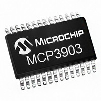
MCP3903T-I/SS Microchip Technology, MCP3903T-I/SS Datasheet - Page 14

MCP3903T-I/SS
Manufacturer Part Number
MCP3903T-I/SS
Description
IC AFE 24BIT 64KSPS 6CH 28SSOP
Manufacturer
Microchip Technology
Series
-r
Datasheet
1.MCP3903-ISS.pdf
(54 pages)
Specifications of MCP3903T-I/SS
Number Of Bits
24
Number Of Channels
6
Power (watts)
-
Voltage - Supply, Analog
4.5 V ~ 5.5 V
Voltage - Supply, Digital
2.7 V ~ 3.6 V
Package / Case
28-SSOP (0.209", 5.30mm Width)
Lead Free Status / Rohs Status
Lead free / RoHS Compliant
MCP3903
3.0
TABLE 3-1:
3.1
This pin is active low and places the entire chip in a
reset state when active.
When RESET=0, all registers are reset to their default
value, no communication can take place, no clock is
distributed inside the part. This state is equivalent to a
POR state.
Since the default state of the ADCs is on, the analog
power consumption when RESET = 0 is equivalent to
when RESET = 1. Only the digital power consumption
is largely reduced because this current consumption is
essentially dynamic and is reduced drastically when
there is no clock running. All the analog biases are
DS25048B-page 14
Pin No.
10
12
13
14
15
16
17
18
19
20
21
22
23
24
25
26
27
28
11
1
2
3
4
5
6
7
8
9
PIN DESCRIPTION
RESET
PIN FUNCTION TABLE
REFIN+/OUT Non-Inverting Voltage Reference Input and Internal Reference Output Pin
Symbol
REFIN-
RESET
OSC1
OSC2
CH0+
CH1+
CH2+
CH3+
CH4+
CH5+
D
DV
AV
A
CH0-
CH1-
CH2-
CH3-
CH4-
CH5-
DRA
DRB
DRC
SDO
SCK
SDI
CS
GND
GND
DD
DD
Analog Power Supply Pin
Non-Inverting Analog Input Pin for Channel 0
Inverting Analog Input Pin for Channel 0
Inverting Analog Input Pin for Channel 1
Non-Inverting Analog Input Pin for Channel 1
Non-Inverting Analog Input Pin for Channel 2
Inverting Analog Input Pin for Channel 2
Inverting Analog Input Pin for Channel 3
Non-Inverting Analog Input Pin for Channel 3
Non-Inverting Analog Input Pin for Channel 4
Inverting Analog Input Pin for Channel 4
Inverting Analog Input Pin for Channel 5
Non-Inverting Analog Input Pin for Channel 5
Inverting Voltage Reference Input Pin
Analog Ground Pin, Return Path for internal analog circuitry
Digital Ground Pin, Return Path for internal digital circuitry
Data Ready Signal Output for channels pair A
Data Ready Signal Output for channels pair B
Data Ready Signal Output for channels pair C
Oscillator Crystal Connection Pin or Clock Input Pin
Oscillator Crystal Connection Pin
Chip Select for Serial Interface
Serial Interface Clock Pin
Serial Interface Data Output Pin
Serial Interface Data Input Pin
Master Reset Logic Input Pin
Digital Power Supply Pin
enabled during a reset so that the part is fully
operational just after a RESET rising edge. This input
is Schmitt triggered.
3.2
DV
within the MCP3903. This pin requires appropriate
bypass capacitors and should be maintained between
2.7V and 3.6V for specified operation.
DD
is the power supply pin for the digital circuitry
Function
Digital V
DD
(DV
© 2011 Microchip Technology Inc.
DD
)


