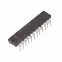
MAX335CNG+ Maxim Integrated Products, MAX335CNG+ Datasheet - Page 6

MAX335CNG+
Manufacturer Part Number
MAX335CNG+
Description
IC SWITCH OCTAL SPST 24DIP
Manufacturer
Maxim Integrated Products
Datasheet
1.MAX335CWG.pdf
(13 pages)
Specifications of MAX335CNG+
Function
Switch
Circuit
8 x SPST - NO
On-state Resistance
150 Ohm
Voltage Supply Source
Dual Supply
Voltage - Supply, Single/dual (±)
±4.5 V ~ 20 V
Operating Temperature
0°C ~ 70°C
Mounting Type
Through Hole
Package / Case
24-DIP (0.300", 7.62mm)
Number Of Switches
Octal
Switch Configuration
SPST
On Resistance (max)
150 Ohms
On Time (max)
400 ns
Off Time (max)
400 ns
Off Isolation (typ)
90 dB
Supply Voltage (max)
+/- 20 V
Supply Voltage (min)
+/- 4.5 V
Supply Current
150 uA
Maximum Power Dissipation
1067 mW
Maximum Operating Temperature
+ 70 C
Mounting Style
Through Hole
Description/function
Analog Switch
Input Level
CMOS, TTL
Minimum Operating Temperature
0 C
Off State Leakage Current (max)
1 nA
Lead Free Status / RoHS Status
Lead free / RoHS Compliant
Serial Controlled, 8-Channel SPST Switch
_____________________Pin Description
Refer to Figure 2. The MAX335 interface can be
thought of as an 8-bit shift register controlled by CS.
While CS is low, input data appearing at DIN is clocked
into the shift register synchronous with SCLK’s rising
edge. The data is an 8-bit word, each bit controlling
one of eight switches in the MAX335 (Table 1). DOUT is
the output of the shift register, with data appearing syn-
chronous with SCLK’s falling edge. Data at DOUT is
simply the input data delayed by eight clock cycles.
When shifting the input data, D7 is the first bit in and
out of the shift register. While shifting data, the switches
remain in their original configuration. When the 8 bits of
data have been shifted in, CS is brought high. This
6
______________Detailed Description
PIN
10
11
12
13
14
15
16
17
18
19
20
21
22
23
24
1
2
3
4
5
6
7
8
9
_______________________________________________________________________________________
COMØ
NAME
COM1
COM2
COM3
COM4
COM5
COM6
COM7
DOUT
SCLK
GND
NOØ
NO1
NO2
NO3
NO4
NO5
NO6
NO7
DIN
C
V+
V
V-
—
S
L
–
Serial Clock Input
Positive Supply Voltage
Serial Data Input
Ground
Switch 0
Switch 0
Switch 1
Switch 1
Switch 2
Switch 2
Switch 3
Switch 3
Switch 4
Switch 4
Switch 5
Switch 5
Switch 6
Switch 6
Switch 7
Switch 7
Negative Supply Voltage
Serial Data Output
Logic Supply/Reset
Chip Select
Serial Digital Interface
FUNCTION
Basic Operation
updates the new switch configuration and inhibits fur-
ther data from entering the shift register. Transitions at
DIN and SCLK have no effect when CS is high, and
DOUT holds the last bit in the shift register.
The MAX335 three-wire serial interface is compatible
with the SPI™ and Microwire™ standards. If interfacing
with a Motorola processor serial interface, set CPOL = 0.
The MAX335 is considered a slave device (Figures 2
and 3). Upon power-up, the shift register contains all
zeros, and all switches are off.
The latch that drives the analog switch is only
updated on the rising edge of
If SCLK is high when
updated until SCLK goes low. The CPOL = 1, CPHA = 1
SPI configuration does not update the latch correctly.
For a simple interface using several MAX335s, “daisy
chain” the shift registers as shown in Figure 5. The CS
pins of all devices are connected together, and a
stream of data is shifted through the MAX335s in
series. When CS is brought high, all switches are
updated simultaneously. Additional shift registers may
be included anywhere in series with the MAX335 data
chain.
When several serial devices are configured as slaves,
addressable by the processor, DIN pins of each
MAX335 are connected together (Figure 6). Address
decode logic individually controls CS of each slave
device. When a slave is selected, its CS is brought low,
data is shifted in, and CS is brought high to latch the
data. Typically, only one slave is addressed at a time.
DOUT is not used.
Digital feedthrough energy measures 100nV-sec, which
means that with no filtering at the signal channel,
feedthrough from a sharply rising clock edge into an
unfiltered switch channel can be measured at 1Vp-p for
100ns. However, even 100pF capacitance in the switch
channel, when combined with the switch resistance,
yields a filter that reduces this transient to 10mVp-p
typical. To reduce digital feedthrough, hysteresis
(150mV typ) was added to the SCLK input so triangle
or sine waves may be used.
CS
Addressable Serial Interface
rises, the latch will not be
CS
Digital Feedthrough
when SCLK is low.
Daisy Chaining


