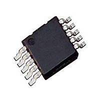
LM4916MMX National Semiconductor, LM4916MMX Datasheet - Page 11

LM4916MMX
Manufacturer Part Number
LM4916MMX
Description
Manufacturer
National Semiconductor
Datasheet
1.LM4916MMX.pdf
(19 pages)
Specifications of LM4916MMX
Operational Class
Class-AB
Audio Amplifier Output Configuration
1-Channel Mono/2-Channel Stereo
Audio Amplifier Function
Headphone/Speaker
Total Harmonic Distortion
0.1@8Ohm@25mW%
Dual Supply Voltage (typ)
Not RequiredV
Power Supply Requirement
Single
Rail/rail I/o Type
No
Power Supply Rejection Ratio
66dB
Single Supply Voltage (min)
900mV
Single Supply Voltage (max)
2.5V
Dual Supply Voltage (min)
Not RequiredV
Dual Supply Voltage (max)
Not RequiredV
Operating Temp Range
-40C to 85C
Operating Temperature Classification
Industrial
Mounting
Surface Mount
Pin Count
10
Package Type
MSOP
Lead Free Status / Rohs Status
Not Compliant
Available stocks
Company
Part Number
Manufacturer
Quantity
Price
Part Number:
LM4916MMX
Manufacturer:
NS/国半
Quantity:
20 000
Typical Performance Characteristics
Application Information
SINGLE ENDED (SE) CONFIGURATION EXPLANATION
As shown in Figure 2, the LM4916 has two operational
amplifiers internally, which have externally configurable gain.
The closed loop gain of the two configurable amplifiers is set
by selecting the ratio of Rf to Ri. Consequently, the gain for
each channel of the IC is
When the LM4916 operates in Single Ended mode, coupling
capacitors are used on each output (VoA and VoB) and the
SE/BTL pin (Pin 8) is connected to ground. These output
coupling capacitors blocks the half supply voltage to which
the output amplifiers are typically biased and couples the
audio signal to the headphones or other single-ended (SE)
loads. The signal return to circuit ground is through the
headphone jack’s sleeve.
BRIDGED (BTL) CONFIGURATION EXPLANATION
As shown in Figure 3, the LM4916 has two internal opera-
tional amplifiers. The first amplifier’s gain is externally con-
figurable, while the second amplifier should be externally
fixed in a unity-gain, inverting configuration. The closed-loop
gain of the first amplifier is set by selecting the ratio of R
R
two external 20kΩ resistors. Figure 3 shows that the output
of amplifier one serves as the input to amplifier two which
results in both amplifiers producing signals identical in mag-
nitude, but out of phase by 180˚. Consequently, the differen-
tial gain for the IC is
By driving the load differentially through outputs Vo1 and
Vo2, an amplifier configuration commonly referred to as
"bridged mode" is established. Bridged mode operation is
different from the classical single-ended amplifier configura-
tion where one side of the load is connected to ground. A
i
while the second amplifier’s gain should be fixed by the
vs Load Resistance
A
Mute Attenuation
A
VD
VD
= 2 *(R
= -(R
f
f
/ R
/ R
i
)
i
).
200487F2
f
to
11
(Continued)
bridge amplifier design has a few distinct advantages over
the single-ended configuration. It provides a differential drive
to the load, thus doubling output swing for a specified supply
voltage. Four times the output power is possible as com-
pared to a single-ended amplifier under the same conditions.
This increase in attainable output power assumes that the
amplifier is not current limited or clipped. In order to choose
an amplifier’s closed-loop gain without causing excessive
clipping, please refer to the Audio Power Amplifier Design
section.
A bridge configuration, such as the one used in LM4916,
also creates a second advantage over single-ended amplifi-
ers. Since the differential outputs, Vo1 and Vo2, are biased
at half-supply, no net DC voltage exists across the load. This
eliminates the need for an output coupling capacitor which is
required in a single supply, single-ended amplifier configura-
tion.
MODE SELECT DETAIL
The LM4916 can be configured in either Single Ended or
BTL mode (see Figure 2 and Figure 3). The default state of
the LM4916 at power up is single ended. During initial power
up or return from shutdown, the LM4916 must detect the
correct mode of operation by sensing the status of the
SE/BTL pin. When the bias voltage of the part ramps up to
60mV (as seen on the Bypass pin), an internal comparator
detects the status of SE/BTL; and at 10mV, latches that
value in place. Ramp up of the bias voltage will proceed at a
different rate from this point on depending upon operating
mode. BTL mode will ramp up about 11 times faster than
Single Ended mode. Shutdown is not a valid command
during this time period (T
ensure a proper power on reset (POR) signal. In addition,
the slew rate of V
reliable POR. Recommended power up timing is shown in
Figure 5 along with proper usage of Shutdown and Mute.
The mode-select circuit is suspended during C
time. The circuit shown in Figure 4 presents an applications
solution to the problem of using different supply voltages
with different turn-on times in a system with the LM4916.
This circuit shows the LM4916 with a 25-50kΩ. Pull-up re-
sistor connected from the shutdown pin to V
DD
Shutdown Current
must be greater than 2.5V/ms to ensure
Distribution
WU
) and should not enabled to
200487F7
DD
B
www.national.com
. The shut-
discharge


