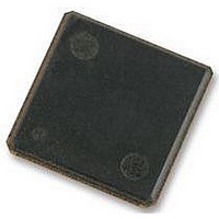
H5PS5162FFR-S6C HYNIX SEMICONDUCTOR, H5PS5162FFR-S6C Datasheet - Page 34

H5PS5162FFR-S6C
Manufacturer Part Number
H5PS5162FFR-S6C
Description
58T1896
Manufacturer
HYNIX SEMICONDUCTOR
Datasheet
1.H5PS5162FFR-S6C.pdf
(39 pages)
Specifications of H5PS5162FFR-S6C
Memory Type
SDRAM
Memory Configuration
32M X 16
Memory Case Style
FBGA
No. Of Pins
84
Operating Temperature Range
0°C To +85°C
Memory Size
512 Mbit
Voltage Vcc
1.8V
Rohs Compliant
Yes
Available stocks
Company
Part Number
Manufacturer
Quantity
Price
Company:
Part Number:
H5PS5162FFR-S6C
Manufacturer:
HYNIX
Quantity:
9 500
Company:
Part Number:
H5PS5162FFR-S6C
Manufacturer:
HYNIX
Quantity:
2 000
Company:
Part Number:
H5PS5162FFR-S6C
Manufacturer:
ST
Quantity:
40
Company:
Part Number:
H5PS5162FFR-S6C
Manufacturer:
HYNIX
Quantity:
4 000
Part Number:
H5PS5162FFR-S6C
Manufacturer:
HYNIX/海力士
Quantity:
20 000
Rev. 1.0 / July. 2008
22. Input waveform timing is referenced from the input signal crossing at the V
nal and V
23. Input waveform timing is referenced from the input signal crossing at the V
nal and V
24. tWTR is at least two clocks (2 x tCK or 2 x nCK) independent of operation frequency.
25. Input waveform timing with single-ended data strobe enabled MR[bit10] = 1, is referenced from the
input signal crossing at the VIH(ac) level to the single-ended data strobe crossing VIH/L(dc) at the start of
its transition for a rising signal, and from the input signal crossing at the VIL(ac) level to the single-ended
data strobe crossing VIH/L(dc) at the start of its transition for a falling signal applied to the device under
test. The DQS signal must be monotonic between Vil(dc)max and Vih(dc)min.
26. Input waveform timing with single-ended data strobe enabled MR[bit10] = 1, is referenced from the
input signal crossing at the VIH(dc) level to the single-ended data strobe crossing VIH/L(ac) at the end of
its transition for a rising signal, and from the input signal crossing at the VIL(dc) level to the single-ended
data strobe crossing VIH/L(ac) at the end of its transition for a falling signal applied to the device under
test. The DQS signal must be monotonic between Vil(dc)max and Vih(dc)min.
27. tCKEmin of 3 clocks means CKE must be registered on three consecutive positive clock edges. CKE
must remain at the valid input level the entire time it takes to achieve the 3 clocks of registration. Thus,
after any CKE transition, CKE may not transition from its valid level during the time period of tIS + 2 x tCK
+ tIH.
IL
IH
(ac) for a falling signal applied to the device under test.
(dc) for a falling signal applied to the device under test.
DQS
DQS
Differential Input waveform timing
tDS
tDH
tDS
tDH
H5PS5162FFR series
V
V
V
V
V
V
V
IH(ac)
IH(dc)
IL(ac)
DDQ
REF
IL(dc)
SS
IH
IL
(dc)
(dc) level for a rising sig-
(ac) level for a rising sig-
max
max
min
min
Release
34


