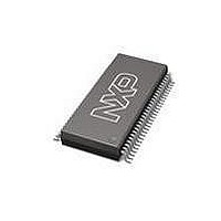
74LVT16652ADL NXP Semiconductors, 74LVT16652ADL Datasheet - Page 7

74LVT16652ADL
Manufacturer Part Number
74LVT16652ADL
Description
Bus Transceivers 3.3V 16-BIT BUS XCVR 3-S
Manufacturer
NXP Semiconductors
Datasheet
1.74LVT16652ADL.pdf
(21 pages)
Specifications of 74LVT16652ADL
Logic Type
BiCMOS
Logic Family
LVT
Number Of Channels Per Chip
16
Input Level
LVTTL
Output Level
LVTTL
Output Type
3-State
High Level Output Current
- 32 mA
Low Level Output Current
64 mA
Propagation Delay Time
2.7 ns
Supply Voltage (max)
3.6 V
Supply Voltage (min)
2.7 V
Maximum Operating Temperature
+ 85 C
Package / Case
SSOP-56
Function
Bus Transceiver / Register
Minimum Operating Temperature
- 40 C
Mounting Style
SMD/SMT
Number Of Circuits
2
Polarity
Non-Inverting
Lead Free Status / Rohs Status
Details
Other names
74LVT16652ADL,512
Available stocks
Company
Part Number
Manufacturer
Quantity
Price
Company:
Part Number:
74LVT16652ADL
Manufacturer:
MAXIM
Quantity:
1 400
Philips Semiconductors
7. Functional description
Table 4:
[1]
[2]
[3]
9397 750 14402
Product data sheet
Operating mode
Isolation
Store A and B data
Store A, hold B
Store A in both registers
Hold A, store B
Store B in both registers
Real-time B data to A bus
Store B data to A bus
Real-time A data to B bus
Store A data to B bus
Stored A data to B bus and
stored B data to A bus
H = HIGH voltage level;
L = LOW voltage level;
X = don’t care;
The data output function may be enabled or disabled by various signals at the nOEBA and nOEAB inputs. Data input functions are
always enabled, i.e., data at the bus pins will be stored on every LOW-to-HIGH transition of the clock.
If both select controls (nSAB and nSBA) are LOW, then clocks can occur simultaneously. If either select control is HIGH, the clocks must
be staggered in order to load both registers.
= LOW-to-HIGH clock transition.
Function table
7.1 Function table
Table 3:
Symbol
V
1B1
1B0
GND
1SBA
1CPBA
1OEBA
CC
[1]
Input
nOEAB nOEBA nCPAB
L
L
X
H
L
L
L
L
H
H
H
Pin description
H
H
H
H
X
L
L
L
H
H
L
Pin
50
51
52
53
54
55
56
H or L
H or L
X
X
X
H or L
H or L
Rev. 03 — 12 January 2005
…continued
Description
supply voltage
data input or output (B-side)
data input or output (B-side)
ground (0 V)
B to A select input
B to A clock input
B to A output enable input
nCPBA nSAB
H or L
H or L
X
H or L
X
X
H or L
X
X
X
X
X
X
X
L
H
H
[3]
3.3 V 16-bit bus transceiver/register; 3-state
nSBA
X
X
X
X
X
L
H
X
X
H
[3]
Data I/O
nAx
input
input
input
input
unspecified
output
unspecified
output
output
output
input
input
output
© Koninklijke Philips Electronics N.V. 2005. All rights reserved.
74LVT16652A
[2]
[2]
nBx
input
input
unspecified
output
unspecified
output
input
input
input
input
output
output
output
[2]
[2]
7 of 21


