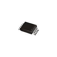
M24C01-RDW6T STMicroelectronics, M24C01-RDW6T Datasheet - Page 20

M24C01-RDW6T
Manufacturer Part Number
M24C01-RDW6T
Description
EEPROM 5.5V 1K (128x8)
Manufacturer
STMicroelectronics
Datasheet
1.M24C16-WMN6TP.pdf
(39 pages)
Specifications of M24C01-RDW6T
Memory Size
1 Kbit
Organization
128 K x 8
Interface Type
I2C
Maximum Clock Frequency
0.4 MHz
Access Time
900 ns
Supply Voltage (max)
5.5 V
Supply Voltage (min)
1.8 V
Maximum Operating Current
0.8 mA
Maximum Operating Temperature
+ 85 C
Mounting Style
SMD/SMT
Package / Case
TSSOP-8
Minimum Operating Temperature
- 40 C
Operating Supply Voltage
6.5 V
Operating Temperature
- 40 C to + 130 C
Lead Free Status / Rohs Status
No
Available stocks
Company
Part Number
Manufacturer
Quantity
Price
Part Number:
M24C01-RDW6TP
Manufacturer:
ST
Quantity:
20 000
DC and AC parameters
20/39
Table 9.
1. The device is not selected after a power-up, after a read command (after the Stop condition), or after the
Table 10.
1. The device is not selected after a power-up, after a read command (after the Stop condition), or after the
Symbol
Symbol
I
V
I
V
I
V
I
CC1
V
V
I
I
completion of the internal write cycle t
CC1
V
completion of the internal write cycle t
I
LO
CC
I
CC
LO
LI
OL
OL
IH
LI
IL
IH
IL
Input leakage current
(SCL, SDA, E0, E1,and E2)
Output leakage current
Supply current
Standby supply current
Input low voltage (SDA,
SCL, WC)
Input high voltage (SDA,
SCL, WC)
Output low voltage
Input leakage current (SCL,
SDA, E0, E1,and E2)
Output leakage current
Supply current
Standby supply current
Input low voltage (SDA,
SCL, WC)
Input high voltage (SDA,
SCL, WC)
Output low voltage
DC characteristics (M24Cxx-W, device grade 6)
DC characteristics (M24Cxx-W, device grade 3)
Parameter
Parameter
Doc ID 5067 Rev 16
W
W
V
Test conditions (in addition to those in
Device not selected
SDA in Hi-Z, external voltage applied on
IN
(t
(t
W
I
W
Device not selected
(in addition to those in
Device not selected
OL
= V
I
OL
is triggered by the correct decoding of a write command).
is triggered by the correct decoding of a write command).
I
SDA in Hi-Z, external voltage
applied on SDA: V
OL
I
V
= 2.1 mA when V
OL
V
SS
= 2.1 mA when V
IN
V
V
CC
= 3 mA when V
(rise/fall time < 50 ns)
(rise/fall time < 50 ns)
V
for 2.5 V < V
CC
CC
= 3 mA when V
or V
= V
(rise/fall time < 50 ns)
(rise/fall time < 50 ns)
or V
CC
or V
M24C16, M24C08, M24C04, M24C02, M24C01
= 2.5 V, f
Test condition
SDA: V
Standby mode
= 5 V, f
= 2.5 V, f
SS
CC
= 5 V, f
CC
CC
or V
, V
Table
, device in Standby mode
, V
CC
C
SS
(1)
CC
C
CC
c
= 400 kHz
c
CC
= 400 kHz
= 400 kHz
, V
= 2.5 V
or V
(1)
(1)
6)
, device in
= 5 V
= 400 kHz
CC
SS
CC
CC
IN
, V
CC
, V
CC
5.5 V
= 2.5 V or
or V
= 5.5 V
= V
Table
IN
IN
= 2.5 V or
= 5.5 V
= V
= V
SS
CC
SS
SS
or V
6)
CC
0.7V
–0.45
Min.
,
0.7V
–0.45 0.3V
CC
Min.
CC
0.3V
V
Max.
CC
± 2
± 2
0.4
V
3
3
5
2
Max. Unit
CC
± 2
± 2
0.4
+1
CC
2
1
1
+1
CC
Unit
mA
mA
µA
µA
µA
µA
mA
mA
V
V
V
µA
µA
µA
V
V
V


