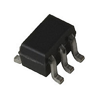
IAM91563TR1 Avago Technologies US Inc., IAM91563TR1 Datasheet - Page 7

IAM91563TR1
Manufacturer Part Number
IAM91563TR1
Description
Manufacturer
Avago Technologies US Inc.
Datasheet
1.IAM91563TR1.pdf
(14 pages)
Specifications of IAM91563TR1
Operating Supply Voltage
3V
Lead Free Status / Rohs Status
Not Compliant
To assist designers in optimizing not only the immedi-
ate circuit using the IAM-9563, but to also optimize and
evaluate trade-offs that affect a complete wireless system,
the standard deviation (σ) is provided for many of the Elec-
trical Specifications parameters (at 5°) in addition to the
mean. The standard deviation is a measure of the variabil-
ity about the mean. It will be recalled that a normal distri-
bution is completely described by the mean and standard
deviation.
Standard statistics tables or calculations provide the prob-
ability of a parameter falling between any two values,
usually symmetrically located about the mean. Referring
to Figure for example, the probability of a parameter
being between ±σ is 68.3%; between ±σ is 95.4%; and
between ±3σ is 99.7%.
Figure 19. Normal Distribution.
Phase Reference Planes
The positions of the reference planes used to specify Re-
flection Coefficients for this device are shown in Figure 0.
As seen in the illustration, the reference planes are located
at the point where the package leads contact the test cir-
cuit.
Figure 20. Phase Reference Planes.
RF Layout
An RF layout similar to the one in Figure is suggested
as a starting point for microstripline designs using the
IAM-9563 mixer. This layout shows the capacitor for the
Source Bypass pin and the optional resistor used to in-
crease bias current. Adequate grounding is important to
obtain maximum performance and to maintain stability.
Both of the ground pins of the MMIC should be connect-
ed to the RF groundplane on the backside of the PCB by
means of plated through holes (vias) that are placed near
the package terminals. As a minimum, one via should be
located next to each of the ground pins to ensure good
RF grounding. It is a good practice to use multiple vias to
further minimize ground path inductance.
7
-3σ
-2σ
TEST CIRCUIT
REFERENCE
PLANES
-1σ
Parameter Value
68%
95%
99%
Mean (µ)
(typical)
+1σ +2σ +3σ
Figure 21. RF Layout.
It is recommended that the PCB pads for the ground pins
not be connected together underneath the body of the
package. PCB traces hidden under the package cannot be
adequately inspected for SMT solder quality.
PCB Material
FR-4 or G-0 printed circuit board materials are a good
choice for most low cost wireless applications. Typi-
cal board thickness is 0.00 to 0.03 inches. Thicknesses
greater than 0.03 inch began to introduce excessive
inductance in the ground vias. The width of the 50Ω mi-
crostriplines on PC boards in this thickness range is also
very convenient for mounting chip components such as
the series inductor at the input or DC blocking and bypass
capacitors.
For applications using higher frequencies such as the 5.8
GHz ISM band, the additional cost of PTFE/glass dielectric
materials may be warranted to minimize transmission line
loss at the mixer’s RF input. An additional consideration
of using lower cost materials at higher frequencies is the
degradation in the Q’s of transmission lines used for im-
pedance matching.
Biasing
The IAM-9563 is a voltage-biased device and is designed
to operate in the “normal mode” from a single, +3 volt
power supply with a typical current drain of only 9 mA.
The internal current regulation circuit allows the mixer to
be operated with voltages as high as +5 volts or as low as
+.5 volt.
The device current can be increased up to 0 mA by
adding an external resistor from the Source Bypass pin
to ground. This feature makes it possible to operate the
IAM-9563 in the “high power mode” to achieve greater
linearity. Refer to the section titled “High Linearity Mode”
for information on applications and performance when
using this feature.


