AD7011ARS Analog Devices Inc, AD7011ARS Datasheet - Page 9
AD7011ARS
Manufacturer Part Number
AD7011ARS
Description
Manufacturer
Analog Devices Inc
Datasheet
1.AD7011ARS.pdf
(12 pages)
Specifications of AD7011ARS
Device Type
Modulator
Modulation Type
Quadrature
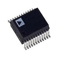
Pin Count
24
Package Type
SSOP
Lead Free Status / Rohs Status
Not Compliant
Available stocks
Company
Part Number
Manufacturer
Quantity
Price

Part Number:
AD7011ARS
Manufacturer:
ADI/亚德诺
Quantity:
20 000
Part Number:
AD7011ARSZ
Manufacturer:
ADI/亚德诺
Quantity:
20 000


REV. B
CIRCUIT DESCRIPTION
TRANSMIT SECTION
The transmit section of the AD7011 generates /4 DQPSK I
and Q waveforms in accordance with TIA specification. This is
accomplished by a digital /4 DQPSK modulator, which
includes the root-raised cosine filters ( = 0.35), followed by
two 10-bit DACs and on-chip reconstruction filters. The /4
DQPSK (Differential Quadrature Phase Shift Keying) digital
modulator generates 10-bit I and Q data in response to the
transmit data stream. The 10-bit I and Q DACs are filtered by
on-chip reconstruction filters, which also generate differential
analog outputs for both I and Q channels.
The AD7011 transmit channel also provides an analog mode,
where direct access to the I and Q DACs is provided, bypassing
the /4 DQPSK modulator. This is provided so that the
AD7011 transmit channel can also be used to perform the
conversion and filtering of the analog waveforms required to
emulate the existing analog cellular system.
The /4 DQPSK modulator generates 10-bit I and Q data
(Inphase and Quadrature) which are loaded into the I and Q
10-bit transmit DACs.
Figure 9 shows the functional block diagram of the /4 DQPSK
modulator. The transmit serial data (TxDATA) is first con-
verted into Di-bit symbols [X
converter. The data is then differentially encoded; symbols are
transmitted as changes in phase rather than absolute phases.
Each symbol represents a phase change, as illustrated in Table
III, and this along with the previously transmitted symbol
determines the next symbol to be transmitted. The differential
phase encoder generates I and Q impulses [I
the Di-bit symbols according to:
Figure 9. /4 DQPSK Modulator Functional Block Diagram
TxDATA
/4 DQPSK Modulator
CONVERTER
SERIAL TO
PARALLEL
2-BIT
X
1
0
0
1
k
X
Y
Q
I
k
k
k
k
/4 DQPSK DIGITAL
= COS [
= SIN [
MODULATOR
DIFFERENTIAL
ENCODER
Table III.
PHASE
k
, Y
Y
1
1
0
0
k
k
], using a 2-bit serial to parallel
k–1
k–1
+
+
Q
I
k
k
COSINE FILTER
COSINE FILTER
k
ROOT-RAISED
ROOT-RAISED
k
]
]
k
3
4
, Q
4
4
3
4
k
k
] in response to
10
10
I DATA
Q DATA
–9–
Figure 10 illustrates the /4 DQPSK constellation diagram as
described above, showing the eight possible states for [I
The I
cosine filters ( = 0.35), generating 10-bit I and Q data. The
FIR root raised cosine filters have an impulse response of 4
symbols.
Transmit Calibration
When the transmit section is brought out of sleep mode
(POWER high), the transmit section initiates a self-calibration
routine to remove the offset between ITx and ITx and an offset
between QTx and QTx. READY goes high on the completion
of the self-calibration routine. Once READY goes high, BIN
(Burst In) can be brought high to initiate a transmit burst.
Ramp-Up/Down Envelope Logic
The AD7011 provides on-chip envelope shaping logic, providing
power shaping control for the beginning and end of a transmit
burst. When BIN (Burst In) is brought high, the modulator is
reset to a transmitting all zeros state (i.e., X
continues to transmit all zeros for the first three symbols, during
which the ramp-up envelope goes from zero to full scale as
illustrated in Figure 11. The next symbol to be transmitted is
[I
BIN going high, i.e., [X
When BIN is brought low, indicating the end of a transmit
burst, the current Di-bit symbol [X
is receiving will be the last symbol to be computed for the four
symbol ramp-down sequence. Also the N
active symbol prior to ramping down.
However, because the impulse response is equal to 4 symbols,
four additional symbols are required to fully compute the analog
outputs when transmitting the (N+4)
be eight subsequent TxCLKs, latching four additional Di-bit
symbols: [X
1
, Q
k
1
], which represents the first two data bits clocked in after
and Q
Figure 10. /4 DQPSK Constellation Diagram
–– – –– COS
1
2
N + 5
k
3 SYMBOLS
impulses are then filtered by FIR raised root
1
2
, Y
Figure 11. Ramp Envelope
N + 5
–––
3T
] to [X
t
1
, Y
1
].
N + 8
Q
, Y
N+4
N + 8
th
, Y
–– + –– COS
symbol. Hence there will
1
2
].
th
N+4
3 SYMBOLS
1
2
symbol is the last
k
] that the AD7011
= Y
AD7011
k
= 0) and
–––
3T
I
t
k
, Q
k
].
Related parts for AD7011ARS
Image
Part Number
Description
Manufacturer
Datasheet
Request
R

Part Number:
Description:
±1.7g Dual-Axis IMEMS Accelerometer Evaluation Board
Manufacturer:
Analog Devices Inc
Datasheet:

Part Number:
Description:
Inertial Sensor Evaluation System
Manufacturer:
Analog Devices Inc
Datasheet:
Part Number:
Description:
Manufacturer:
Analog Devices Inc
Datasheet:
Part Number:
Description:
Manufacturer:
Analog Devices Inc
Datasheet:
Part Number:
Description:
Manufacturer:
Analog Devices Inc
Datasheet:
Part Number:
Description:
Manufacturer:
Analog Devices Inc
Datasheet:
Part Number:
Description:
Manufacturer:
Analog Devices Inc
Datasheet:
Part Number:
Description:
Manufacturer:
Analog Devices Inc
Datasheet:
Part Number:
Description:
Manufacturer:
Analog Devices Inc
Datasheet:
Part Number:
Description:
Manufacturer:
Analog Devices Inc
Datasheet:
Part Number:
Description:
Manufacturer:
Analog Devices Inc
Datasheet:
Part Number:
Description:
Manufacturer:
Analog Devices Inc
Datasheet:
Part Number:
Description:
Manufacturer:
Analog Devices Inc
Datasheet: