LM4665LD National Semiconductor, LM4665LD Datasheet
LM4665LD
Specifications of LM4665LD
Available stocks


Related parts for LM4665LD

LM4665LD Summary of contents
Page 1
... The LM4665 has short circuit protection against a short from the outputs GND or across the outputs. DD Typical Application FIGURE 1. Typical Audio Amplifier Application Circuit Boomer ® registered trademark of National Semiconductor Corporation. © 2002 National Semiconductor Corporation Key Specifications j Efficiency at 100mW into 8Ω transducer j Efficiency at 400mW into 8Ω transducer j ...
Page 2
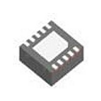
... Connection Diagrams Mini Small Outline (MSOP) Package Top View Order Number LM4665MM See NS Package Number MUB10A LLP Package Top View Order Number LM4665LD See NS Package Number LDA10B micro SMD Marking Top View X - Date Code T- Die Traceability G - Boomer Family A2 - LM4665ITL www.national.com 20027023 ...
Page 3
... Absolute Maximum Ratings 2) If Military/Aerospace specified devices are required, please contact the National Semiconductor Sales Office/ Distributors for availability and specifications. Supply Voltage (Note 1) Storage Temperature + 0.3V ≥ V ≥ GND - 0.3V Voltage at Any Input Pin V DD Power Dissipation (Note 3) ESD Susceptibility (Note 4) ...
Page 4
Electrical Characteristics V The following specifications apply for V erwise specified. Limits apply for T A Symbol Parameter I Quiescent Power Supply Current DD I Shutdown Current SD V Shutdown Voltage Input High SDIH V Shutdown Voltage Input Low SDIL ...
Page 5
Typical Performance Characteristics THD+N vs Frequency 8Ω + 33µ 400mW, 30kHz BW OUT THD+N vs Frequency V = 3.3V 4Ω + 33µ 300mW, 30kHz BW ...
Page 6
Typical Performance Characteristics THD+N vs Common-Mode Voltage 8Ω + 33µ 1kHz 400mW, 22kHz BW OUT CMRR vs Frequency 8Ω + 33µ ...
Page 7
Typical Performance Characteristics PSRR vs Frequency 8Ω + 33µ 100mV Sine Wave, 22kHz BW CM RMS Efficiency (top trace) and Power Dissipation (bottom trace) vs Output Power V = 5V, R ...
Page 8
Typical Performance Characteristics Output Power vs Supply Voltage R = 16Ω + 33µ 1kHz L Output Power vs Supply Voltage R = 4Ω + 33µ 1kHz L Shutdown Hysteresis Voltage V = 3V, SD Mode = ...
Page 9
Typical Performance Characteristics Shutdown Hysteresis Voltage V = 3V, SD Mode = GND (SD High) DD Application Information GENERAL AMPLIFIER FUNCTION The output signals generated by the LM4665 consist of two, BTL connected, output signals that pulse momentarily from near ...
Page 10
Application Information the output pins to the load and the supply pins to the power supply should be as wide as possible to minimize trace resistance. The rising and falling edges are necessarily short in relation to the minimum pulse ...
Page 11
Application Information FIGURE 2. Increased Supply Voltage Operating Range for the micro SMD package SINGLE-ENDED CIRCUIT CONFIGURATIONS FIGURE 3. Single-Ended Input, Shutdown High and Gain of 6dB Configuration (Continued) 11 200270E5 200270C4 www.national.com ...
Page 12
Application Information FIGURE 4. Single-Ended Input, Shutdown High and Gain of 12dB Configuration FIGURE 5. Single-Ended Input, Shutdown Low and Gain of 6dB Configuration www.national.com (Continued) 12 200270C2 200270C3 ...
Page 13
Application Information FIGURE 6. Single-Ended Input, Shutdown Low and Gain of 12dB Configuration REFERENCE DESIGN BOARD SCHEMATIC (Continued) FIGURE 7. 13 200270C1 200270B1 www.national.com ...
Page 14
Application Information In addition to the minimal parts required for the application circuit, a measurement filter is provided on the evaluation circuit board so that conventional audio measurements can be conveniently made without additional equipment. This is a balanced input ...
Page 15
Application Information LM4665 LLP BOARD ARTWORK Composite View Top Layer (Continued) 200270D1 200270D3 15 Silk Screen 200270D2 Bottom Layer 200270D4 www.national.com ...
Page 16
Application Information LM4665 micro SMD BOARD ARTWORK Composite View Top Layer www.national.com (Continued) 200270C7 200270B9 16 Silk Screen 200270C8 Bottom Layer 200270C0 ...
Page 17
Physical Dimensions inches (millimeters) unless otherwise noted 9 Bump micro SMD Order Number LM4665ITL, LM4665ITLX NS Package Number TLA09AAA X = 1.514 X = 1.514 X = 0.600 Mini Small Outline (MSOP) Order Number LM4665MM NSPackage Number ...
Page 18
... National does not assume any responsibility for use of any circuitry described, no circuit patent licenses are implied and National reserves the right at any time without notice to change said circuitry and specifications. inches (millimeters) unless otherwise noted (Continued) LLP Order Number LM4665LD NSPackage Number LDA10B 2. A critical component is any component of a life ...