PC451T Sharp Electronics, PC451T Datasheet
PC451T
Specifications of PC451T


Related parts for PC451T


PC451T Summary of contents
Page 1
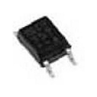
PC451 Series ■ Description PC451 Series contains an IRED optically coupled to a phototransistor packaged in a 4-pin Mini-flat. Input-output isolation voltage(rms) is 3.75kV. Collector-emitter voltage is 350V. CTR is MIN. 40% at input current of 5mA. ■ ...
Page 2
Internal Connection Diagram 1 2 ■ Outline Dimensions ±0.3 3.6 ±0.25 2. Date code SHARP mark "s" Anode mark ±0 0.4 Epoxy resin Anode 1 4 Cathode 2 Emitter 3 3 Collector ...
Page 3
Date code (2 digit) 1st digit Year of production A.D. Mark A.D Mark 1990 A 2002 P 1991 B 2003 R 1992 C 2004 S 1993 D 2005 T 1994 E 2006 U 1995 F 2007 V 1996 H 2008 ...
Page 4
Absolute Maximum Ratings Parameter Symbol Forward current I F Reverse voltage V R Power dissipation P Collector-emitter voltage V CEO Emitter-collector voltage V ECO Collector current I C Collector power dissipation P C Total power dissipation P tot Operating ...
Page 5
... Model Line-up Taping Package 3 000 pcs/reel 750 pcs/reel Model No. PC451 PC451T Please contact a local SHARP sales representative to inquire about production status and Lead-Free options. 5 PC451 Series Sheet No.: D2-A00301EN ...
Page 6
Fig.1 Forward Current vs. Ambient Temperature − Ambient temperature T Fig.3 Collector Power Dissipation vs. Ambient Temperature 200 150 100 50 0 − Ambient temperature T ...
Page 7
Fig.7 Current Transfer Ratio vs. Forward Current 100 Forward current I F Fig.9 Relative Current Transfer Ratio vs. Ambient Temperature 150 100 50 0 − Ambient temperature T Fig.11 Collector Dark ...
Page 8
Fig.13 Test Circuit for Response Time Input Output Output Input Please refer to the conditions in Fig.12 Fig.15 Test Circuit for Frequency Response R D Please refer to ...
Page 9
Design Considerations ● Design guide While operating at I <1.0mA, CTR variation may increase. F Please make design considering this fact. This product is not designed against irradiation and incorporates non-coherent IRED. ● Degradation In general, the emission of ...
Page 10
Manufacturing Guidelines ● Soldering Method Reflow Soldering: Reflow soldering should follow the temperature profile shown below. Soldering should not exceed the curve of temperature profile and time. Please don't solder more than twice. (˚C) 300 Terminal : 260˚C peak ...
Page 11
Cleaning instructions Solvent cleaning: Solvent temperature should be 45˚C or below Immersion time should be 3minutes or less Ultrasonic cleaning: The impact on the device varies depending on the size of the cleaning bath, ultrasonic output, cleaning time, size ...
Page 12
Package specification ● Tape and Reel package 1. 3 000pcs/reel Package materials Carrier tape : A-PET (with anti-static material) Cover tape : PET (three layer system) Reel : PS Carrier tape structure and Dimensions F Dimensions List A ±0.3 ...
Page 13
Package materials Carrier tape : A-PET (with anti-static material) Cover tape : PET (three layer system) Reel : PS Carrier tape structure and Dimensions F Dimensions List A B ±0.3 ±0.1 12.0 5 ...
Page 14
Important Notices · The circuit application examples in this publication are provided to explain representative applications of SHARP devices and are not intended to guarantee any circuit design or license any intellectual property rights. SHARP takes no responsibility for ...