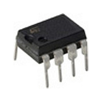
M24C01-BN6 STMicroelectronics, M24C01-BN6 Datasheet - Page 13

M24C01-BN6
Manufacturer Part Number
M24C01-BN6
Description
Manufacturer
STMicroelectronics
Datasheet
1.M24C01-BN6.pdf
(40 pages)
Specifications of M24C01-BN6
Density
1Kb
Interface Type
Serial (I2C)
Organization
128x8
Access Time (max)
900ns
Frequency (max)
400KHz
Write Protection
Yes
Data Retention
40Year
Operating Supply Voltage (typ)
5V
Package Type
PDIP
Operating Temp Range
-40C to 85C
Supply Current
2mA
Operating Supply Voltage (min)
4.5V
Operating Supply Voltage (max)
5.5V
Operating Temperature Classification
Industrial
Mounting
Through Hole
Pin Count
8
Lead Free Status / Rohs Status
Not Compliant
Available stocks
Company
Part Number
Manufacturer
Quantity
Price
M24C16, M24C08, M24C04, M24C02, M24C01
3.5
Memory addressing
To start communication between the bus master and the slave device, the bus master must
initiate a Start condition. Following this, the bus master sends the device select code, shown
in
The device select code consists of a 4-bit Device Type Identifier, and a 3-bit Chip Enable
“Address” (E2, E1, E0). To address the memory array, the 4-bit Device Type Identifier is
1010b.
Each device is given a unique 3-bit code on the Chip Enable (E0, E1, E2) inputs. When the
device select code is received, the device only responds if the Chip Enable Address is the
same as the value on the Chip Enable (E0, E1, E2) inputs. However, those devices with
larger memory capacities (the M24C16, M24C08 and M24C04) need more address bits. E0
is not available for use on devices that need to use address line A8; E1 is not available for
devices that need to use address line A9, and E2 is not available for devices that need to
use address line A10 (see
up to eight M24C02 (or M24C01), four M24C04, two M24C08 or one M24C16 devices can
be connected to one I²C bus. In each case, and in the hybrid cases, this gives a total
memory capacity of 16 Kbits, 2 KBytes (except where M24C01 devices are used).
The 8
If a match occurs on the device select code, the corresponding device gives an
acknowledgment on Serial Data (SDA) during the 9
the device select code, it deselects itself from the bus, and goes into Standby mode.
Table 4.
1. X =
Current Address Read
Random Address Read
Sequential Read
Byte Write
Page Write
Table 3
th
V
IH
bit is the Read/Write bit (RW). This bit is set to 1 for Read and 0 for Write operations.
or V
Mode
(on Serial Data (SDA), most significant bit first).
IL
Operating modes
.
RW bit
Figure 2
1
0
1
1
0
0
Doc ID 5067 Rev 13
and
WC
V
V
X
X
X
X
IL
IL
(1)
Table 3
Bytes
for details). Using the E0, E1 and E2 inputs,
1
1
1
16
1
th
bit time. If the device does not match
Start, Device Select, RW = 1
Start, Device Select, RW = 0, Address
reStart, Device Select, RW = 1
Similar to Current or Random Address
Read
Start, Device Select, RW = 0
Start, Device Select, RW = 0
Initial sequence
Device operation
13/40


