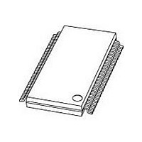
74ALVCH16244DGG NXP Semiconductors, 74ALVCH16244DGG Datasheet - Page 2

74ALVCH16244DGG
Manufacturer Part Number
74ALVCH16244DGG
Description
Manufacturer
NXP Semiconductors
Datasheet
1.74ALVCH16244DGG.pdf
(20 pages)
Specifications of 74ALVCH16244DGG
Logic Family
ALVC
Logical Function
Buffer/Line Driver
Number Of Elements
4
Number Of Channels
16
Number Of Inputs
16
Number Of Outputs
16
Operating Supply Voltage (typ)
1.8/2.5/3.3V
Package Type
TSSOP
Output Type
3-State
Polarity
Non-Inverting
Propagation Delay Time
7.1ns
High Level Output Current
-24mA
Low Level Output Current
24mA
Operating Supply Voltage (max)
3.6V
Operating Supply Voltage (min)
1.2V
Quiescent Current
40uA
Technology
CMOS
Pin Count
48
Mounting
Surface Mount
Operating Temp Range
-40C to 85C
Operating Temperature Classification
Industrial
Lead Free Status / Rohs Status
Compliant
Available stocks
Company
Part Number
Manufacturer
Quantity
Price
Company:
Part Number:
74ALVCH16244DGG
Manufacturer:
Philips
Quantity:
12 495
Part Number:
74ALVCH16244DGG
Manufacturer:
NXP/恩智浦
Quantity:
20 000
Company:
Part Number:
74ALVCH16244DGGRG4
Manufacturer:
PHILIPS
Quantity:
5
Philips Semiconductors
FEATURES
QUICK REFERENCE DATA
GND = 0 V; T
Notes
1. C
2. The condition is V
2003 May 14
t
C
C
PHL
Wide supply voltage range from 1.2 to 3.6 V
CMOS low power consumption
MultiByte flow-through standard pin-out architecture
Low inductance multiple V
noise and ground bounce
Direct interface with TTL levels
Bus hold on data inputs (74ALVCH16244 only)
Output drive capability 50
Current drive 24 mA at 3.0 V
Complies with JEDEC standard no. 8-1 A
ESD protection:
HBM EIA/JESD22-A114-A exceeds 2000 V
MM EIA/JESD22-A115-A exceeds 200 V.
I
PD
2.5 V/3.3 V 16-bit buffer/line driver
(3-state)
SYMBOL
P
f
f
C
V
N = total load switching outputs;
i
o
/t
(C
D
CC
PD
= input frequency in MHz;
L
PLH
= output frequency in MHz;
= output load capacitance in pF;
= C
L
is used to determine the dynamic power dissipation (P
= supply voltage in Volts;
PD
V
CC
amb
2
propagation delay nAn to nYn
input capacitance
power dissipation capacitance per buffer
V
= 25 C; t
CC
f
o
2
) = sum of the outputs.
I
f
= GND to V
i
N + (C
r
CC
= t
PARAMETERS
f
transmission lines at 85 C
and GND pins for minimum
2.5 ns
L
CC
.
V
CC
2
f
o
) where:
2
V
V
notes 1 and 2
DESCRIPTION
The 74ALVC16244; 74ALVCH16244 is a 16-bit
non-inverting buffer/line driver with 3-state outputs. The
device can be used as four 4-bit buffers, two 8-bit buffers
or one 16-bit buffer. The 3-state outputs are controlled by
the output enable inputs 1OE, 2OE, 3OE and 4OE. A
HIGH on nOE causes the outputs to assume a
high-impedance OFF-state.
The 74ALVCH16244 has active bus hold circuitry which is
provided to hold unused or floating data inputs at a valid
logic level. This feature eliminates the need for external
pull-up or pull-down resistors.
The 74ALVC16244 has 5 V tolerant inputs.
CC
CC
outputs enabled
outputs disabled
D
= 2.5 V; C
= 3.3 V; C
in W).
CONDITIONS
L
L
= 30 pF
= 50 pF
1.9
1.9
5.0
25
4
74ALVCH16244
TYPICAL
74ALVC16244;
Product specification
ns
ns
pF
pF
pF
UNIT


