CY7C1019CV33-15ZC Cypress Semiconductor Corp, CY7C1019CV33-15ZC Datasheet
CY7C1019CV33-15ZC
Specifications of CY7C1019CV33-15ZC


Related parts for CY7C1019CV33-15ZC

CY7C1019CV33-15ZC Summary of contents
Page 1
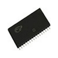
... I/O pins. The eight input/output pins (I/O high-impedance state when the device is deselected (CE HIGH), the outputs are disabled (OE HIGH), or during a write operation (CE LOW, and WE LOW). The CY7C1019CV33 is available in Standard 48-ball FBGA, 32-pin TSOP II and 400-mil-wide SOJ packages I/O 0 I/O 1 ...
Page 2
... Pin Configuration Selection Guide Maximum Access Time Maximum Operating Current Maximum Standby Current Note pins are not connected on the die. Document #: 38-05130 Rev. *F 48-ball VFBGA (Top View I/O NC I -10 - CY7C1019CV33 -15 Unit Page [+] Feedback ...
Page 3
... MAX , 5 CC – 0.3V, CC > V – 0.3V, CC < 0.3V Test Conditions T = 25° MHz 5.0V CC CY7C1019CV33 Ambient Temperature V CC 3.3V ± 10% 0°C to +70°C 3.3V ± 10% –40°C to +85°C –12 –15 Min. Max. Min. Max. Unit 2.4 2.4 0.4 ...
Page 4
... The minimum write cycle time for Write Cycle no. 3 (WE controlled, OE LOW) is the sum of t Document #: 38-05130 Rev. *F [4] ALL INPUT PULSES 90% 90% 10% (b) Fall Time: 1 V/ns [5] -10 Min. Max. Min less than less than t , and t HZCE LZCE HZOE LZOE and t HZWE CY7C1019CV33 High-Z characteristics: R 317Ω 3.3V 10% OUTPUT 5 pF (c) -12 -15 Max. Min. Max. Unit ...
Page 5
... Data I/O is high impedance 15 goes HIGH simultaneously with WE going HIGH, the output remains in a high-impedance state. Document #: 38-05130 Rev OHA DOE DATA VALID 50 SCE SA t SCE PWE t SD DATA VALID CY7C1019CV33 DATA VALID t HZOE t HZCE HIGH IMPEDANCE t PD ICC 50% ISB Page [+] Feedback ...
Page 6
... During this period the I/Os are in the output state and input signals should not be applied. Document #: 38-05130 Rev. *F [14, 15 SCE PWE t SD DATA VALID IN [15 SCE PWE t SD DATA VALID Mode 7 Power-Down Read Write Selected, Outputs Disabled CY7C1019CV33 LZWE Power Standby ( Active ( Active ( Active ( Page [+] Feedback ...
Page 7
... Ordering Code 10 CY7C1019CV33-10VC CY7C1019CV33-10ZXC CY7C1019CV33-10ZXI 12 CY7C1019CV33-12VC CY7C1019CV33-12ZC CY7C1019CV33-12ZXC CY7C1019CV33-12VI CY7C1019CV33-12BVXI 15 CY7C1019CV33-15VC CY7C1019CV33-15VXC CY7C1019CV33-15ZXC CY7C1019CV33-15ZXI Package Diagrams Document #: 38-05130 Rev. *F Package Diagram Package Type 51-85033 32-pin 400-Mil Molded SOJ 51-85095 32-pin TSOP II (Pb-Free) 32-pin TSOP II (Pb-Free) 51-85033 32-pin 400-Mil Molded SOJ ...
Page 8
... Package Diagrams (continued) Document #: 38-05130 Rev. *F 32-pin TSOP II (51-85095) CY7C1019CV33 51-85095-** Page [+] Feedback ...
Page 9
... The inclusion of Cypress products in life-support systems application implies that the manufacturer assumes all risk of such use and in doing so indemnifies Cypress against all charges. 48-ball VFBGA ( mm) (51-85150) A CY7C1019CV33 BOTTOM VIEW A1 CORNER Ø0. Ø ...
Page 10
... Document History Page Document Title: CY7C1019CV33 128K x 8 Static RAM Document Number: 38-05130 Issue REV. ECN NO. Date ** 109245 12/16/01 *A 113431 04/10/02 *B 115047 08/01/02 *C 119796 10/11/02 *D 123030 12/17/02 *E 419983 See ECN *F 493543 See ECN Document #: 38-05130 Rev. *F Orig. of Change Description of Change HGK ...