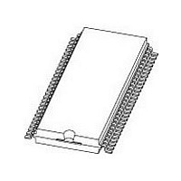
PCF8576CT NXP Semiconductors, PCF8576CT Datasheet - Page 17

PCF8576CT
Manufacturer Part Number
PCF8576CT
Description
Manufacturer
NXP Semiconductors
Datasheet
1.PCF8576CT.pdf
(56 pages)
Specifications of PCF8576CT
Operating Supply Voltage (typ)
2.5/3.3/5V
Number Of Digits
20
Number Of Segments
160
Package Type
VSO
Pin Count
56
Mounting
Surface Mount
Power Dissipation
400mW
Frequency (max)
315KHz
Operating Supply Voltage (min)
2V
Operating Supply Voltage (max)
6V
Lead Free Status / Rohs Status
Compliant
Available stocks
Company
Part Number
Manufacturer
Quantity
Price
Part Number:
PCF8576CT
Manufacturer:
PHILIPS/飞利浦
Quantity:
20 000
Part Number:
PCF8576CT/1
Manufacturer:
NXP/恩智浦
Quantity:
20 000
Part Number:
PCF8576CT/1,518
Manufacturer:
NXP/恩智浦
Quantity:
20 000
Company:
Part Number:
PCF8576CT/1112
Manufacturer:
NXP Semiconductors
Quantity:
135
Company:
Part Number:
PCF8576CT/1118
Manufacturer:
NXPSemicondu
Quantity:
2 802
Company:
Part Number:
PCF8576CT/1Ј¬112
Manufacturer:
NXP
Quantity:
880
Company:
Part Number:
PCF8576CT/1Ј¬118
Manufacturer:
NXP
Quantity:
21 000
Part Number:
PCF8576CT/F1
Manufacturer:
PHILIPS/飞利浦
Quantity:
20 000
Part Number:
PCF8576CTT
Manufacturer:
NXP/恩智浦
Quantity:
20 000
NXP Semiconductors
PCF8576C_9
Product data sheet
7.5.1 Internal clock
7.5.2 External clock
7.5 Oscillator
7.6 Timing
The internal logic and the LCD drive signals of the PCF8576C are timed by the frequency
f
f
The clock frequency (f
for data reception from the I
rate of 100 kHz, f
The internal oscillator is enabled by connecting pin OSC to pin V
output from pin CLK is the clock signal for any cascaded PCF8576s or PCF8566s in the
system.
Remark: The PCF8576C is backwards compatible with the PCF8576 (V
Where resistor R
Connecting pin OSC to V
external clock input.
Remark: A clock signal must always be supplied to the device. Removing the clock,
freezes the LCD in a DC state, which is not suitable for the liquid crystal.
The timing of the PCF8576C sequences the internal data flow of the device. This includes
the transfer of display data from the display RAM to the display segment outputs. In
cascaded applications, the synchronization signal (SYNC) maintains the correct timing
relationship between the PCF8576Cs in the system. The timing also generates the LCD
frame frequency which is derived as an integer division of the clock frequency (see
Table
used or by the frequency applied to the pin CLK when an external clock is used.
Table 6.
[1]
[2]
[3]
The ratio between the clock frequency and the LCD frame frequency depends on the
mode in which the device is operating. In the power-saving mode the reduction ratio is six
times smaller; this allows the clock frequency to be reduced by a factor of six. The
reduced clock frequency results in a significant reduction in power consumption.
PCF8576C mode
Normal mode
Power saving mode
clk
clk(ext)
, which equals either the built-in oscillator frequency f
The possible values for f
For f
For f
6). The frame frequency is set by the mode set commands when an internal clock is
.
clk
clk
= 200 kHz.
= 31 kHz.
LCD frame frequencies
ext
clk
(on pin OSC) to V
should be chosen to be above 125 kHz.
clk
clk
) determines the LCD frame frequency (f
Rev. 09 — 9 July 2009
DD
see
2
enables an external clock source. Pin CLK then becomes the
C-bus. To allow I
Frame frequency
f
f
Table
fr
fr
=
=
[1]
20.
------------ -
2880
--------- -
480
f
f
clk
clk
SS
is present, the internal oscillator is selected.
Universal LCD driver for low multiplex rates
2
C-bus transmissions at their maximum data
osc
Nominal frame frequency (Hz)
69
65
or the external clock frequency
[2]
[3]
fr
SS
) and the maximum rate
. In this case, the
PCF8576C
© NXP B.V. 2009. All rights reserved.
oper
up to 9 V).
17 of 56


