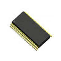
IDT74LVCHR16646APA IDT, Integrated Device Technology Inc, IDT74LVCHR16646APA Datasheet - Page 3

IDT74LVCHR16646APA
Manufacturer Part Number
IDT74LVCHR16646APA
Description
Manufacturer
IDT, Integrated Device Technology Inc
Datasheet
1.IDT74LVCHR16646APA.pdf
(8 pages)
Specifications of IDT74LVCHR16646APA
Logic Family
LVC
Operating Supply Voltage (typ)
3.3V
Propagation Delay Time
8.5ns
Number Of Elements
2
Number Of Channels
16
Input Logic Level
LVTTL
Output Logic Level
LVTTL
Output Type
3-State
Package Type
TSSOP
Polarity
Non-Inverting
Logical Function
Bus Transceiver/Register
Operating Supply Voltage (min)
2.7V
Operating Supply Voltage (max)
3.6V
Technology
CMOS
Operating Temp Range
-40C to 85C
Operating Temperature Classification
Industrial
Mounting
Surface Mount
Pin Count
56
Lead Free Status / Rohs Status
Not Compliant
Available stocks
Company
Part Number
Manufacturer
Quantity
Price
Company:
Part Number:
IDT74LVCHR16646APA
Manufacturer:
IDT
Quantity:
6 234
NOTES:
1. H = HIGH Voltage Level
2. The data output functions may be enabled or disabled by various signals at OE or DIR. Data input functions are always enabled, i.e. data at the bus pins will be stored
DC ELECTRICAL CHARACTERISTICS OVER OPERATING RANGE
Following Conditions Apply Unless Otherwise Specified:
Operating Condition: T
NOTES:
1. Typical values are at V
2. This applies in the disabled state only.
FUNCTION TABLE
IDT74LVCHR16646A
3.3V CMOS 16-BIT BUS TRANSCEIVER/REGISTER WITH 3-STATE OUTPUTS
X = Don’t Care
L = LOW Voltage Level
↑ = LOW-to-HIGH transition
on every LOW-to-HIGH transition of the clock inputs.
Symbol
xOE
∆I
I
I
I
I
I
I
V
V
OZH
OFF
V
CCH
CCZ
OZL
V
CCL
I
H
H
I
X
X
L
L
L
L
IH
IL
CC
IH
IL
IK
H
Input HIGH Voltage Level
Input LOW Voltage Level
Input Leakage Current
High Impedance Output Current
(3-State Output pins)
Input/Output Power Off Leakage
Clamp Diode Voltage
Input Hysteresis
Quiescent Power Supply Current
Quiescent Power Supply Current
Variation
xDIR
H
H
X
X
X
X
L
L
A
CC
= –40°C to +85°C
Parameter
= 3.3V, +25°C ambient.
xCLKAB
H or L
H or L
↑
↑
X
X
X
X
Inputs
(1)
xCLKBA
H or L
H or L
↑
↑
X
X
X
X
V
V
V
V
V
V
V
V
V
V
One input at V
CC
CC
CC
CC
CC
CC
CC
CC
CC
CC
= 2.3V to 2.7V
= 2.7V to 3.6V
= 2.3V to 2.7V
= 2.7V to 3.6V
= 0V, V
= 2.3V, I
= 3.6V
= 3.6V
= 3.3V
= 3.6V
xSAB
H
X
X
X
X
X
X
L
IN
IN
CC
or V
= –18mA
- 0.6V, other inputs at V
O
≤
xSBA
Test Conditions
5.5V
H
X
X
X
X
X
X
L
3
Unspecified
Output
Output
Input
Input
Input
Input
Input
V
V
V
3.6
xAx
I
O
IN
= 0 to 5.5V
CC
= 0 to 5.5V
= GND or V
≤
V
Data I/O
or GND
IN
≤
5.5V
Unspecified
(2)
CC
(2)
Output
Output
Input
Input
Input
Input
Input
xBx
INDUSTRIAL TEMPERATURE RANGE
Min.
1.7
—
—
—
—
—
—
—
—
—
—
2
Store A, B unspecified
Store B, A unspecified
Store A and B data
Isolation, hold storage
Real time B data to A bus
Stored B data to A bus
Real time A data to B bus
Stored A data to B bus
Typ.
Operation or Function
–0.7
100
—
—
—
—
—
—
—
—
—
—
(1)
Max.
–1.2
±10
±50
500
0.7
0.8
±5
(2)
(2)
—
—
—
10
10
Unit
µA
µA
µA
mV
µA
µA
V
V
V


