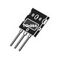
APT10035LLLG MICROSEMI, APT10035LLLG Datasheet - Page 2

APT10035LLLG
Manufacturer Part Number
APT10035LLLG
Description
Manufacturer
MICROSEMI
Type
Power MOSFETr
Datasheet
1.APT10035LLLG.pdf
(5 pages)
Specifications of APT10035LLLG
Number Of Elements
1
Polarity
N
Channel Mode
Enhancement
Drain-source On-res
0.35Ohm
Drain-source On-volt
1kV
Gate-source Voltage (max)
±30V
Continuous Drain Current
28A
Operating Temp Range
-55C to 150C
Operating Temperature Classification
Military
Mounting
Through Hole
Pin Count
3 +Tab
Package Type
TO-264
Lead Free Status / Rohs Status
Compliant
Available stocks
Company
Part Number
Manufacturer
Quantity
Price
Company:
Part Number:
APT10035LLLG
Manufacturer:
APT
Quantity:
10 000
DYNAMIC CHARACTERISTICS
SOURCE-DRAIN DIODE RATINGS AND CHARACTERISTICS
THERMAL CHARACTERISTICS
APT Reserves the right to change, without notice, the specifications and information contained herein.
1 Repetitive Rating: Pulse width limited by maximum junction
2 Pulse Test: Pulse width < 380 µs, Duty Cycle < 2%
3 See MIL-STD-750 Method 3471
Symbol
Symbol
Symbol
t
R
R
C
t
C
dv
temperature
C
V
Q
Q
d(off)
E
E
Q
d(on)
E
E
I
Q
t
SM
I
oss
t
t
SD
rss
S
iss
on
off
on
off
gd
rr
/
gs
r
f
JC
g
JA
rr
dt
0.20
0.15
0.10
0.05
0
Characteristic / Test Conditions
Continuous Source Current (Body Diode)
Pulsed Source Current
Diode Forward Voltage
Reverse Recovery Time (I
Reverse Recovery Charge (I
Peak Diode Recovery
Characteristic
Input Capacitance
Output Capacitance
Reverse Transfer Capacitance
Total Gate Charge
Gate-Source Charge
Gate-Drain ("Miller ") Charge
Turn-on Delay Time
Rise Time
Turn-off Delay Time
Fall Time
Turn-on Switching Energy
Turn-off Switching Energy
Turn-on Switching Energy
Turn-off Switching Energy
Characteristic
Junction to Case
Junction to Ambient
10
-5
FIGURE 1, MAXIMUM EFFECTIVE TRANSIENT THERMAL IMPEDANCE, JUNCTION-TO-CASE vs PULSE DURATION
0.9
0.7
0.5
0.3
0.1
0.05
10
3
-4
dv
2
1
/
dt
(V
S
(Body Diode)
6
6
5
= -I
GS
S
SINGLE PULSE
= -I
D
= 0V, I
28A
RECTANGULAR PULSE DURATION (SECONDS)
D
28A
, dl
S
, dl
S
= -I
10
/dt = 100A/µs)
-3
S
D
/dt = 100A/µs)
28A
INDUCTIVE SWITCHING @ 125°C
INDUCTIVE SWITCHING @ 25°C
)
V
RESISTIVE SWITCHING
V
4 Starting T
5
6 Eon includes diode reverse recovery. See figures 18, 20.
DD
Test Conditions
DD
I
I
D
D
I
I
dv
device itself.
D
D
= 670V, V
= 28A, R
= 28A, R
= 670V V
V
= 28A @ 25°C
V
= 28A @ 25°C
/
V
V
V
dt
R
V
f = 1 MHz
DD
DD
DS
GS
GS
G
GS
numbers reflect the limitations of the test circuit rather than the
= 1.6
= 500V
= 500V
= 25V
= 15V
= 10V
= 0V
10
G
G
GS
j
-2
GS
= +25°C, L = 7.50mH, R
= 5
= 5
= 15V
= 15V
I
S
-
I
D
28A
Note:
Peak T J = P DM x Z JC + T C
di
MIN
/
MIN
Duty Factor D = t 1 / t
MIN
dt
10
-1
700A/µs
t 1
G
t 2
= 25 , Peak I
16.28
5185
1423
1170
TYP
881
160
186
122
900
623
779
TYP
TYP
24
12
10
36
APT10035 B2LL - LLL
9
V
2
R
V
MAX
DSS
MAX
MAX
0.18
100
1.3
40
25
10
1.0
L
= 28A
T
J
150
Amps
UNIT
UNIT
Volts
UNIT
°C/W
V/ns
nC
µC
pF
ns
µ
ns
°
J
C


