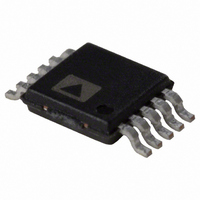
ADG1421BRMZ Analog Devices Inc, ADG1421BRMZ Datasheet - Page 14

ADG1421BRMZ
Manufacturer Part Number
ADG1421BRMZ
Description
IC SW SPST 2.1OHM RON 10MSOP
Manufacturer
Analog Devices Inc
Series
iCMOS®r
Datasheet
1.ADG1423BRMZ.pdf
(16 pages)
Specifications of ADG1421BRMZ
Function
Switch
Circuit
2 x SPST - NO
On-state Resistance
6.2 Ohm
Voltage Supply Source
Dual, Single, Dual Supply
Voltage - Supply, Single/dual (±)
±5V, 12V, ±15V
Current - Supply
120µA
Operating Temperature
-40°C ~ 125°C
Mounting Type
Surface Mount
Package / Case
10-TFSOP, 10-MSOP (0.118", 3.00mm Width)
Analog Switch Type
SPST
No. Of Channels
2
Bandwidth
180MHz
On State Resistance Max
2.1ohm
Turn Off Time
115ns
Turn On Time
115ns
Supply Voltage Range
13.5V To 16.5V
Lead Free Status / RoHS Status
Lead free / RoHS Compliant
Available stocks
Company
Part Number
Manufacturer
Quantity
Price
Company:
Part Number:
ADG1421BRMZ
Manufacturer:
Analog Devices Inc
Quantity:
135
Part Number:
ADG1421BRMZ
Manufacturer:
ADI/亚德诺
Quantity:
20 000
Part Number:
ADG1421BRMZ-REEL7
Manufacturer:
ADI/亚德诺
Quantity:
20 000
ADG1421/ADG1422/ADG1423
TERMINOLOGY
I
The positive supply current.
I
The negative supply current.
V
The analog voltage on Terminal D and Terminal S.
R
The ohmic resistance between Terminal D and Terminal S.
R
Flatness is defined as the difference between the maximum and
minimum value of on resistance as measured over the specified
analog signal range.
I
The source leakage current with the switch off.
I
The drain leakage current with the switch off.
I
The channel leakage current with the switch on.
V
The maximum input voltage for Logic 0.
V
The minimum input voltage for Logic 1.
I
The input current of the digital input.
C
The off switch source capacitance, measured with reference to
ground.
C
The off switch drain capacitance, measured with reference to
ground.
C
The on switch capacitance, measured with reference to ground.
C
The digital input capacitance.
DD
SS
S
D
D
INL
ON
FLAT (ON)
S
D
D
IN
D
INL
INH
, I
(Off)
(Off)
, C
(Off)
(V
(Off)
(I
S
(On)
S
INH
S
)
(On)
)
Rev. 0 | Page 14 of 16
t
Delay time between the 50% and 90% points of the digital input
and switch on condition. See Figure 26.
t
Delay time between the 50% and 90% points of the digital input
and switch off condition. See Figure 26.
t
Delay time between the 50% and 90% points of the digital
inputs and the switch on condition when switching from one
address state to another.
T
Off time measured between the 80% point of both switches
when switching from one address state to another. See Figure 27.
Charge Injection
A measure of the glitch impulse transferred from the digital
input to the analog output during switching. See Figure 28.
Off Isolation
A measure of unwanted signal coupling through an off switch.
See Figure 29.
Crosstalk
A measure of unwanted signal that is coupled through from one
channel to another as a result of parasitic capacitance. See
Figure 30.
Bandwidth
The frequency at which the output is attenuated by 3 dB. See
Figure 31.
On Response
The frequency response of the on switch.
Insertion Loss
The loss due to the on resistance of the switch. See Figure 31.
THD + N
The ratio of the harmonic amplitude plus noise of the signal to
the fundamental. See Figure 32.
AC Power Supply Rejection Ratio (ACPSRR)
ACPSRR measures the ability of a part to avoid coupling noise
and spurious signals that appear on the supply voltage pin to the
output of the switch. The dc voltage on the device is modulated
by a sine wave of 0.62 V p-p. The ratio of the amplitude of signal on
the output to the amplitude of the modulation is the ACPSRR.
See Figure 22.
ON
OFF
TRANSITION
BBM
(EN)
(EN)


