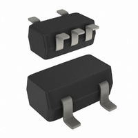
74LVC1G66GW,125 NXP Semiconductors, 74LVC1G66GW,125 Datasheet - Page 12

74LVC1G66GW,125
Manufacturer Part Number
74LVC1G66GW,125
Description
IC SWITCH SPST 5TSSOP
Manufacturer
NXP Semiconductors
Series
74LVCr
Type
Analog Switchr
Datasheet
1.74LVC1G66GM115.pdf
(25 pages)
Specifications of 74LVC1G66GW,125
Package / Case
6-TSSOP (5 lead), SC-88A, SOT-353
Function
Switch
Circuit
1 x SPST- NO
On-state Resistance
6 Ohm
Voltage Supply Source
Single Supply
Voltage - Supply, Single/dual (±)
1.65 V ~ 5.5 V
Current - Supply
0.1µA
Operating Temperature
-40°C ~ 125°C
Mounting Type
Surface Mount
Switch Configuration
SPST
On Resistance (max)
34 Ohm (Typ) @ 1.95 V
On Time (max)
5.3 ns (Typ) @ 1.95 V
Off Time (max)
4.2 ns (Typ) @ 1.95 V
Supply Voltage (max)
5.5 V
Supply Voltage (min)
1.65 V
Maximum Power Dissipation
250 mW
Maximum Operating Temperature
+ 125 C
Mounting Style
SMD/SMT
Minimum Operating Temperature
- 40 C
Switch Current (typ)
0.0001 mA @ 3.3 V
Multiplexer Configuration
Single SPST
Number Of Inputs
1
Number Of Outputs
1
Number Of Channels
1
Analog Switch On Resistance
34@1.95VOhm
Package Type
TSSOP
Power Supply Requirement
Single
Single Supply Voltage (min)
1.65V
Single Supply Voltage (typ)
3/5V
Single Supply Voltage (max)
5.5V
Dual Supply Voltage (min)
Not RequiredV
Dual Supply Voltage (typ)
Not RequiredV
Dual Supply Voltage (max)
Not RequiredV
Power Dissipation
250mW
Mounting
Surface Mount
Pin Count
5
Operating Temp Range
-40C to 125C
Operating Temperature Classification
Automotive
Lead Free Status / RoHS Status
Lead free / RoHS Compliant
Lead Free Status / RoHS Status
Lead free / RoHS Compliant, Lead free / RoHS Compliant
Other names
568-4614-2
74LVC1G66GW-G
74LVC1G66GW-G
935269058125
74LVC1G66GW-G
74LVC1G66GW-G
935269058125
NXP Semiconductors
Table 11.
Table 12.
At recommended operating conditions; voltages are referenced to GND (ground = 0 V); T
74LVC1G66
Product data sheet
Supply voltage
V
1.65 V to 1.95 V
2.3 V to 2.7 V
2.7 V
3.0 V to 3.6 V
4.5 V to 5.5 V
Symbol
THD
Fig 18. Test circuit for measuring switching times
CC
Test data is given in
Definitions for test circuit:
R
C
R
V
T
L
L
EXT
Test data
Additional dynamic characteristics
= Load capacitance including jig and probe capacitance.
= Load resistance.
= Termination resistance should be equal to output impedance Z
Parameter
total harmonic distortion
= External voltage for measuring switching times.
11.2 Additional dynamic characteristics
Input
V
V
V
2.7 V
2.7 V
V
Table
I
CC
CC
CC
11.
t
≤ 2.0 ns
≤ 2.0 ns
≤ 2.5 ns
≤ 2.5 ns
≤ 2.5 ns
r
, t
G
All information provided in this document is subject to legal disclaimers.
f
Conditions
R
see
R
see
L
L
V
V
V
V
V
V
V
V
= 10 kΩ; C
= 10 kΩ; C
CC
CC
CC
CC
CC
CC
CC
CC
Figure 19
Figure 19
V
I
= 1.65 V
= 2.3 V
= 3.0 V
= 4.5 V
= 1.65 V
= 2.3 V
= 3.0 V
= 4.5 V
Rev. 7 — 30 July 2010
Load
C
30 pF
30 pF
50 pF
50 pF
50 pF
L
R T
L
L
DUT
V
= 50 pF; f
= 50 pF; f
CC
R
1 kΩ
500 Ω
500 Ω
500 Ω
500 Ω
V
L
O
i
i
= 1 kHz;
= 10 kHz;
o
of the pulse generator.
C L
V
V
t
open
open
open
open
open
mna616
EXT
PLH
EXT
R L
R L
, t
PHL
amb
Min
-
-
-
-
-
-
-
-
= 25
t
GND
GND
GND
GND
GND
PZH
74LVC1G66
Typ
0.032
0.008
0.006
0.001
0.068
0.009
0.008
0.006
, t
°
C.
PHZ
© NXP B.V. 2010. All rights reserved.
Bilateral switch
Max
-
-
-
-
-
-
-
-
t
2V
2V
6 V
6 V
2V
PZL
CC
CC
CC
, t
PLZ
Unit
%
%
%
%
%
%
%
%
12 of 25


