MM74HC4066M Fairchild Semiconductor, MM74HC4066M Datasheet

IC SWITCH 1X1 14SOIC

MM74HC4066M

Manufacturer Part Number
MM74HC4066M
Description
IC SWITCH 1X1 14SOIC
Manufacturer
Fairchild Semiconductor
Series
74HCr
Datasheets

Specifications of MM74HC4066M

Function
Switch
Circuit
1 x 1:1
On-state Resistance
70 Ohm
Voltage Supply Source
Single Supply
Voltage - Supply, Single/dual (±)
2 V ~ 12 V
Current - Supply
8µA
Operating Temperature
-40°C ~ 85°C
Mounting Type
Surface Mount
Package / Case
14-SOIC (0.154", 3.90mm Width)
Lead Free Status / RoHS Status
Lead free / RoHS Compliant

Available stocks

Company
Part Number
Manufacturer
Quantity
Price
Part Number:
MM74HC4066M
Manufacturer:
TI/德州仪器
Quantity:
20 000
Part Number:
MM74HC4066MTC
Manufacturer:
FairchildSem
Quantity:
2 802
Part Number:
MM74HC4066MTCX
Manufacturer:
LATTICE
Quantity:
115
Part Number:
MM74HC4066MTCX
Manufacturer:
FAIRCHILD
Quantity:
2 261
Part Number:
MM74HC4066MX
Manufacturer:
FAIRCHIL
Quantity:
4 237
Part Number:
MM74HC4066MX
Quantity:
56
Part Number:
MM74HC4066MX
Manufacturer:
FAIRCHILD/仙童
Quantity:
20 000
© 2000 Fairchild Semiconductor Corporation
MM74HC4066M
MM74HC4066SJ
MM74HC4066MTC
MM74HC4066N
MM74HC4066
Quad Analog Switch
General Description
The MM74HC4066 devices are digitally controlled analog
switches utilizing advanced silicon-gate CMOS technology.
These switches have low “ON” resistance and low “OFF”
leakages. They are bidirectional switches, thus any analog
input may be used as an output and visa-versa. Also the
MM74HC4066 switches contain linearization circuitry
which lowers the “ON” resistance and increases switch lin-
earity. The MM74HC4066 devices allow control of up to
12V (peak) analog signals with digital control signals of the
same range. Each switch has its own control input which
disables each switch when LOW. All analog inputs and out-
puts and digital inputs are protected from electrostatic
damage by diodes to V
Ordering Code:
Devices also available in Tape and Reel. Specify by appending the suffix letter “X” to the ordering code.
Schematic Diagram
Truth Table
Order Number
Package Number
CC
MTC14
and ground.
M14A
M14D
N14A
14-Lead Small Outline Integrated Circuit (SOIC), JEDEC MS-120, 0.150” Narrow
14-Lead Small Outline Package (SOP), EIAJ TYPE II, 5.3mm Wide
14-Lead Thin Shrink Small Outline Package (TSSOP), JEDEC MO-153, 4.4mm Wide
14-Lead Plastic Dual-In-Line Package (PDIP), JEDEC MS-001, 0.300” Wide
Input
DS005355
CTL
H
L
Features
Connection Diagram
Typical switch enable time: 15 ns
Wide analog input voltage range: 0–12V
Low “ON” resistance: 30 typ. (MM74HC4066)
Low quiescent current: 80 A maximum (74HC)
Matched switch characteristics
Individual switch controls
Switch
I/O–O/I
“OFF”
Package Description
“ON”
Top View
August 1984
Revised January 2000
www.fairchildsemi.com

Related parts for MM74HC4066M

MM74HC4066M Summary of contents

Page 1

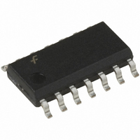
... M14A 14-Lead Small Outline Integrated Circuit (SOIC), JEDEC MS-120, 0.150” Narrow MM74HC4066SJ M14D 14-Lead Small Outline Package (SOP), EIAJ TYPE II, 5.3mm Wide MM74HC4066MTC MTC14 14-Lead Thin Shrink Small Outline Package (TSSOP), JEDEC MO-153, 4.4mm Wide MM74HC4066N N14A 14-Lead Plastic Dual-In-Line Package (PDIP), JEDEC MS-001, 0.300” Wide Devices also available in Tape and Reel. Specify by appending the suffix letter “ ...

Page 2

Absolute Maximum Ratings (Note 2) Supply Voltage ( Control Input Voltage ( Switch I/O Voltage ( Clamp Diode Current ( Output Current, per pin ...

Page 3

AC Electrical Characteristics V = 2.0V 6. 12V (unless otherwise specified Symbol Parameter Conditions Maximum Propagation PHL PLH Delay Switch In to Out Maximum ...

Page 4

AC Test Circuits and Switching Time Waveforms FIGURE 1. “ON” Resistance FIGURE 3. “OFF” Channel Leakage Current FIGURE PHL PLH FIGURE PZL PLZ FIGURE PZH PHZ www.fairchildsemi.com FIGURE ...

Page 5

AC Test Circuits and Switching Time Waveforms FIGURE 8. Crosstalk: Control Input to Signal Output FIGURE 9. Crosstalk Between Any Two Switches FIGURE 10. Switch OFF Signal Feedthrough Isolation (Continued) FIGURE 7. Frequency Response FIGURE 11. Sinewave Distortion 5 www.fairchildsemi.com ...

Page 6

Typical Performance Characteristics Typical “ON” Resistance Special Considerations In certain applications the external load-resistor current may include both V and signal line components avoid drawing V current when switch current flows into CC www.fairchildsemi.com Typical Crosstalk Between Any ...

Page 7

Physical Dimensions inches (millimeters) unless otherwise noted 14-Lead Small Outline Integrated Circuit (SOIC), JEDEC MS-120, 0.150” Narrow Package Number M14A 7 www.fairchildsemi.com ...

Page 8

Physical Dimensions inches (millimeters) unless otherwise noted (Continued) 14-Lead Small Outline Package (SOP), EIAJ TYPE II, 5.3mm Wide www.fairchildsemi.com Package Number M14D 8 ...

Page 9

Physical Dimensions inches (millimeters) unless otherwise noted (Continued) 14-Lead Thin Shrink Small Outline Package (TSSOP), JEDEC MO-153, 4.4mm Wide Package Number MTC14 9 www.fairchildsemi.com ...

Page 10

Physical Dimensions inches (millimeters) unless otherwise noted (Continued) 14-Lead Plastic Dual-In-Line Package (PDIP), JEDEC MS-001, 0.300” Wide Fairchild does not assume any responsibility for use of any circuitry described, no circuit patent licenses are implied and Fairchild reserves the right ...

Related keywords