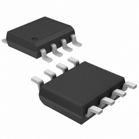
MAX4529ESA+ Maxim Integrated Products, MAX4529ESA+ Datasheet - Page 7

MAX4529ESA+
Manufacturer Part Number
MAX4529ESA+
Description
IC VIDEO SWITCH SPST 8SOIC
Manufacturer
Maxim Integrated Products
Datasheet
1.MAX4529CUTT.pdf
(12 pages)
Specifications of MAX4529ESA+
Function
Video Switch
Circuit
1 x SPST- NC
On-state Resistance
120 Ohm
Voltage Supply Source
Single, Dual Supply
Voltage - Supply, Single/dual (±)
2.7 V ~ 12 V, ± 2.7 V ~ 6 V
Current - Supply
50µA
Operating Temperature
-40°C ~ 85°C
Mounting Type
Surface Mount
Package / Case
8-SOIC (0.154", 3.90mm Width)
Lead Free Status / RoHS Status
Lead free / RoHS Compliant
The MAX4529 is constructed as a high-frequency “T”
switch, as shown in Figure 1. The logic-level input, IN,
is translated by amplifier A1 into a V+ to V- logic signal
that drives inverter A2. Amplifier A2 drives the gates of
N-channel MOSFETs N1 and N2 from V+ to V-, turning
them fully on or off. The same signal drives inverter A3
(which drives the P-channel MOSFETs P1 and P2) from
V+ to V-, turning them fully on or off, and drives the N-
channel MOSFET N3 off and on.
The logic-level threshold is determined by V+ and
GND. The voltage on GND is usually at ground poten-
tial, but it may be set to any voltage between
(V+ - 2V) and V-. When the voltage between V+ and
GND is less than 2V, the level translators become very
slow and unreliable. Normally, GND should be connect-
ed to the ground plane.
When the switch is on, MOSFETs N1, N2, P1, and P2
are on and MOSFET N3 is off. The signal path is COM to
NC, and because both N-channel and P-channel
MOSFETs act as pure resistances, it is symmetrical (i.e.,
signals may pass in either direction). The off MOSFET,
N3, has no DC conduction, but has a small amount of
capacitance to GND. The four on MOSFETs also have
capacitance to ground that, together with the series
resistance, forms a lowpass filter. All of these capaci-
*
** NC and COM pins are identical and interchangeable. Either may be considered as an input or output; signals pass equally well in
SOT23-6
All pins except N.C. have ESD diodes to V- and V+.
either direction.
—
1
2
3
4
5
6
PIN
DIP/SO/µMAX
_______________________________________________________________________________________
1, 6
2
8
5
4
3
7
Theory of Operation
Logic-Level Translators
Switch On Condition
NAME
COM
GND
N.C.
NC
V+
IN
V-
Not Internally Connected
Analog Switch Normally Closed** Terminal
Positive Supply-Voltage Input (analog and digital). The voltage difference between
V+ and V- should never exceed 12V.
-5V Supply Input. Connect to GND for single-supply operation.
Logic-Level Control Input. Logic-level voltages should never exceed V+ or V-.
RF and Logic Ground. Connect to ground plane.
Analog Switch Common** Terminal. Analog signal voltages should never exceed
V+ or V-.
Low-Voltage, Bidirectional
Figure 1. T-Switch Construction
tances are distributed evenly along the series resis-
tance, so they act as a transmission line rather than a
simple R-C filter. This helps to explain the exceptional
300MHz bandwidth when the switches are on.
Typical attenuation in 50Ω systems is -2dB and is rea-
sonably flat up to 100MHz. Higher-impedance circuits
show even lower attenuation (and vice versa), but
slightly lower bandwidth due to the increased effect of
the internal and external capacitance and the switch’s
internal resistance.
COM
GND
IN
0
1
V+
V-
IN
COM - NC
OFF
ON
A1
FUNCTION*
NORMALLY CLOSED SWITCH CONSTRUCTION
RF/Video Switch
D
A2
N1
S
S
A3
P1
Pin Description
D
D
S
N3
COM, AND NC
D
ESD DIODES
ON GND, IN,
S
N2
P2
S
D
V+
V-
NC
7


