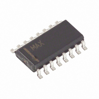
MAX308ESE+ Maxim Integrated Products, MAX308ESE+ Datasheet - Page 6

MAX308ESE+
Manufacturer Part Number
MAX308ESE+
Description
IC MULTIPLEXER 8X1 16SOIC
Manufacturer
Maxim Integrated Products
Type
Analog Multiplexerr
Datasheet
1.MAX308CPE.pdf
(12 pages)
Specifications of MAX308ESE+
Function
Multiplexer
Circuit
1 x 8:1
On-state Resistance
100 Ohm
Voltage Supply Source
Single, Dual Supply
Voltage - Supply, Single/dual (±)
5 V ~ 30 V, ± 5 V ~ 20 V
Operating Temperature
-40°C ~ 85°C
Mounting Type
Surface Mount
Package / Case
16-SOIC (0.154", 3.90mm Width)
Package
16SOIC N
Maximum On Resistance
175@12V Ohm
Maximum Propagation Delay Bus To Bus
175@±15V|450@12V ns
Maximum High Level Output Current
30 mA
Multiplexer Architecture
8:1
Maximum Turn-off Time
300@12V ns
Maximum Turn-on Time
600@12V ns
Power Supply Type
Single|Dual
Product
Multiplexer
Number Of Lines (input / Output)
8.0 / 1.0
Supply Voltage (max)
30 V
Supply Voltage (min)
5 V
Maximum Operating Temperature
+ 85 C
Minimum Operating Temperature
- 40 C
Mounting Style
SMD/SMT
Number Of Input Lines
8.0
Number Of Output Lines
1.0
Power Dissipation
696 mW
Lead Free Status / RoHS Status
Lead free / RoHS Compliant
Using supply voltages less than ±15V will reduce the
analog signal range. The MAX308/MAX309 switches
operate with ±5V to ±20V bipolar supplies or with a
+5V to +30V single supply. Connect V- to GND when
operating with a single supply. Both device types can
also operate with unbalanced supplies, such as +24V
and -5V. The Typical Operating Characteristics graphs
show typical on-resistance with 20V, 15V, 10V, and 5V
supplies. (Switching times increase by a factor of two
or more for operation at 5V.)
Proper power-supply sequencing is recommended for
all CMOS devices. Do not exceed the absolute maxi-
mum ratings, because stresses beyond the listed rat-
ings may cause permanent damage to the devices.
Always sequence V+ on first, then V-, followed by the
logic inputs, NO, or COM. If power-supply sequencing
is not possible, add two small signal diodes in series
with supply pins for overvoltage protection (Figure 1).
Adding diodes reduces the analog signal range to 1V
below V+ and 1V above V-, but does not affect the
devices’ low switch resistance and low leakage charac-
teristics. Device operation is unchanged, and the differ-
ence between V+ and V- should not exceed +44V.
Precision, 8-Channel/Dual 4-Channel,
High-Performance, CMOS Analog Multiplexers
6
______________________________________________________________Pin Description
__________Applications Information
_______________________________________________________________________________________
MAX308
1, 15, 16
9–12
4–7
—
—
—
—
13
14
2
3
8
PIN
Supply Voltages Other than 15V
MAX309
10–13
1, 16
8, 9
4–7
14
15
—
—
—
—
2
3
Overvoltage Protection
COMA, COMB
NO1A–NO4A
NO4B–NO1B
Operation with
A0, A2, A1
NO1–NO4
NO8–NO5
NAME
A0, A1
COM
GND
EN
V+
V-
Address Inputs
Address Inputs
Enable Input
Negative Supply Voltage Input
Analog Inputs—Bidirectional
Analog Inputs—Bidirectional
Analog Output—Bidirectional
Analog Outputs—Bidirectional
Analog Inputs—Bidirectional
Analog Inputs—Bidirectional
Positive Supply Voltage Input
Ground
Figure 1. Overvoltage Protection Using External Blocking
Diodes
V
g
NO
FUNCTION
V+
V-
COM


