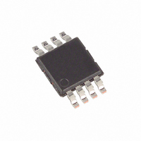
MAX4656EUA+ Maxim Integrated Products, MAX4656EUA+ Datasheet - Page 7

MAX4656EUA+
Manufacturer Part Number
MAX4656EUA+
Description
IC SWITCH SPST 8UMAX
Manufacturer
Maxim Integrated Products
Datasheet
1.MAX4658ESA.pdf
(12 pages)
Specifications of MAX4656EUA+
Function
Switch
Circuit
1 x SPST- NO
On-state Resistance
10 Ohm
Voltage Supply Source
Single, Dual Supply
Voltage - Supply, Single/dual (±)
9 V ~ 40 V, ±4.5 V ~ 20 V
Operating Temperature
-40°C ~ 85°C
Mounting Type
Surface Mount
Package / Case
8-TSSOP, 8-MSOP (0.118", 3.00mm Width)
Number Of Switches
Single
Switch Configuration
SPST
On Resistance (max)
15 Ohms
On Time (max)
300 ns
Off Time (max)
150 ns
Off Isolation (typ)
- 77 dB
Bandwidth
210 MHz
Supply Voltage (max)
20 V
Supply Voltage (min)
4.5 V
Supply Current
90 uA
Maximum Power Dissipation
362 mW
Maximum Operating Temperature
+ 85 C
Mounting Style
SMD/SMT
Minimum Operating Temperature
- 40 C
Off State Leakage Current (max)
10 nA
Lead Free Status / RoHS Status
Lead free / RoHS Compliant
The MAX4655–MAX4658 are single SPST CMOS ana-
log switches. The CMOS switch construction provides
rail-to-rail signal handling while consuming very little
power. The switch is controlled by a TTL/CMOS level
compatible digital input. The MAX4655/MAX4657 are
normally closed switches, and the MAX4656/MAX4658
are normally open switches.
These devices can be operated with either single
power supplies or dual power supplies. Operation at up
to ±20V supplies allows users a wide switching dynamic
range. Additionally, asymmetrical operation is possible
to tailor performance to a particular application.
These switches have been specifically designed to
handle high switch currents, up to 400mA peak current
and 300mA continuous currents. In order to do this, a
new technique is used to drive the body of the output
N-channel device. (Note: the basic switch between the
input NC/NO terminal, and the output common terminal
consists of an N-channel MOSFET and a P-channel
MOSFET in parallel.) The standard method limits opera-
tion to approximately a 600mV drop across the switch.
More than 600mV causes an increase in Id
current (due to the turn-on of on-chip parasitic diodes)
and an increase in V+ supply current. With the new
sensing method, there is no limitation to the voltage
drop across the switch. Current and voltage are limited
only by the power dissipation rating of the package and
the absolute maximum ratings of the switch.
When the analog input to output voltage drop is
approximately 7mV there is an increase in power sup-
ply current from typically 90µA to 2mA within a 1mV to
7mV range, caused by the new sensing/driving circuitry.
Figure 1. Overvoltage Protection Using Blocking Diodes
V g
NO_
_______________________________________________________________________________________
Detailed Description
V+
V-
V+
V-
High-Current, 10 , SPST, CMOS
COM_
ON
leakage
Proper power-supply sequencing is recommended for
all CMOS devices. Do not exceed the absolute maxi-
mum ratings, because stresses beyond the listed rat-
ings can cause permanent damage to the devices.
First, connect GND, followed by V+, V-, and the remain-
ing pins. If power-supply sequencing is not possible,
add two small signal diodes (D1, D2) in series with sup-
ply pins (Figure 1). Adding diodes reduces the analog
signal range to one diode drop below V+ and one
diode drop above V-, but does not affect the devices’
low switch resistance and low leakage characteristics.
Device operation is unchanged, and the difference
between V+ and V- should not exceed 44V. The protec-
tion diode for the negative supply is not required when
V- is connected to GND.
In 50
these parts extends from DC to above 100MHz, with a
typical loss of -2dB. When the switch is turned off, how-
ever, it behaves like a capacitor, and off-isolation
decreases with increasing frequency. This effect is
more pronounced with higher source and load imped-
ances. Above 5MHz, circuit board layout becomes
critical. The graphs shown in the Typical Operating
Characteristics were taken using a 50
load connected with BNC connectors.
systems, the high-frequency on-response of
Off-Isolation at High Frequencies
Analog Switches
Applications Information
Overvoltage Protection
source and
7


