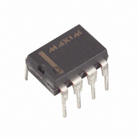
MAX318CPA+ Maxim Integrated Products, MAX318CPA+ Datasheet - Page 6

MAX318CPA+
Manufacturer Part Number
MAX318CPA+
Description
IC SWITCH SPST 8DIP
Manufacturer
Maxim Integrated Products
Datasheet
1.MAX318CPA.pdf
(12 pages)
Specifications of MAX318CPA+
Function
Switch
Circuit
1 x SPST- NO
On-state Resistance
35 Ohm
Voltage Supply Source
Single, Dual Supply
Voltage - Supply, Single/dual (±)
10 V ~ 30 V, ±4.5 V ~ 20 V
Current - Supply
1µA
Operating Temperature
0°C ~ 70°C
Mounting Type
Through Hole
Package / Case
8-DIP (0.300", 7.62mm)
Number Of Switches
Dual
Switch Configuration
SPST
On Resistance (max)
35 Ohms
On Time (max)
175 ns
Off Time (max)
145 ns
Off Isolation (typ)
68 dB
Supply Voltage (max)
+/- 20 V
Supply Voltage (min)
+/- 4.5 V
Supply Current
0.0001 uA
Maximum Power Dissipation
727 mW
Maximum Operating Temperature
+ 70 C
Mounting Style
Through Hole
Description/function
Analog Switch
Input Level
CMOS, TTL
Minimum Operating Temperature
0 C
Off State Leakage Current (max)
6 nA
Lead Free Status / RoHS Status
Lead free / RoHS Compliant
Precision, CMOS Analog Switches
The main limitation of supply voltages other than ±15V
is analog signal range reduction. The MAX317/
MAX318/MAX319 switches operate with bipolar sup-
plies of ±5V to ±20V. Typical Operating Characteristics
graphs show typical on resistance for ±15V, ±10V, and
±5V supplies. Switching times increase by a factor of
two
MAX317/MAX318/MAX319 can operate from unipolar
supplies of +10V to +30V. Both parts can also operate
from unbalanced supplies such as +24V and -5V.
Connect V- to 0V when operating with a single supply.
This means that VL must be connected to +5V to be
TTL compatible, or to V+ for CMOS logic input levels.
Proper power-supply sequencing is recommended for
all CMOS devices. It is important not to exceed the
absolute maximum ratings because stresses beyond
the listed ratings may cause permanent damage to the
devices. Always sequence V+ on first, followed by VL,
V-, and logic inputs. If power-supply sequencing is not
possible, protect the devices from overvoltage by
6
__________Applications Information
MAX317
_______________________________________________________________________Pin Description
_______________________________________________________________________________________
—
—
1
2
3
4
5
6
7
8
or
more
MAX318
Operation with Supply Voltages
PIN
—
—
1
2
3
4
5
6
7
8
for
MAX319
operation
—
—
Overvoltage Protection
1
8
3
4
5
6
7
2
NAME
Other Than ±15V
COM
GND
N.C.
NO
NC
NO
V+
VL
IN
V-
at
Analog-switch common terminal
No connect — not internally connected
Analog-switch normally open terminal
Logic ground
Analog-signal positive supply input
Logic-level positive supply input
Logic-level input
Analog-signal negative supply input
Analog-switch normally closed terminal
Analog-switch normally open terminal
±5V.
The
adding two small signal diodes in series with the sup-
ply pins (Figure 1). Adding the diodes reduces the
analog signal range to 1V below V+ and 1V below V-,
but low switch resistance and low leakage characteris-
tics are unaffected. Device operation is unchanged,
and the difference between V+ to V- should not exceed
+44V.
Figure 1. Overvoltage Protection Using Blocking Diodes
V g
FUNCTION
NO_
V+
V-
V+
V-
COM_


