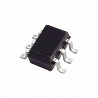
ADG779BKSZ-REEL7 Analog Devices Inc, ADG779BKSZ-REEL7 Datasheet - Page 7

ADG779BKSZ-REEL7
Manufacturer Part Number
ADG779BKSZ-REEL7
Description
IC SWITCH SPDT SC70-6
Manufacturer
Analog Devices Inc
Datasheet
1.ADG779BKSZ-REEL7.pdf
(12 pages)
Specifications of ADG779BKSZ-REEL7
Function
Switch
Circuit
1 x SPDT
On-state Resistance
5 Ohm
Voltage Supply Source
Single Supply
Voltage - Supply, Single/dual (±)
1.8 V ~ 5.5 V
Current - Supply
0.001µA
Operating Temperature
-40°C ~ 85°C
Mounting Type
Surface Mount
Package / Case
6-TSSOP, SC-88, SOT-363
Analog Switch Type
SPDT
No. Of Channels
1
Bandwidth
200MHz
On State Resistance Max
2.5ohm
Turn Off Time
3ns
Turn On Time
14ns
Supply Voltage Range
1.8V To 5.5V
Lead Free Status / RoHS Status
Lead free / RoHS Compliant
Other names
ADG779BKSZ-REEL7TR
Available stocks
Company
Part Number
Manufacturer
Quantity
Price
Company:
Part Number:
ADG779BKSZ-REEL7
Manufacturer:
AD
Quantity:
14 500
Company:
Part Number:
ADG779BKSZ-REEL7
Manufacturer:
Exar
Quantity:
118
Part Number:
ADG779BKSZ-REEL7
Manufacturer:
ADI/亚德诺
Quantity:
20 000
TERMINOLOGY
V
Most positive power supply potential.
I
Positive supply current.
GND
Ground (0 V) reference.
S
Source terminal. Can be an input or an output.
D
Drain terminal. Can be an input or an output.
IN
Logic control input.
V
Analog voltage on drain (D) and source (S) terminals.
R
Ohmic resistance between the D and S.
R
Flatness is defined as the difference between the maximum and
minimum value of on resistance as measured.
ΔR
On-resistance mismatch between any two channels.
I
Source leakage current with the switch off.
I
Drain leakage current with the switch off.
I
Channel leakage current with the switch on.
V
Maximum input voltage for Logic 0.
V
Minimum input voltage for Logic 1.
I
Input current of the digital input.
C
Off switch source capacitance. Measured with reference to
ground.
DD
S
D
D
INL
ON
FLAT (ON)
S
DD
D
INL
INH
, I
(Off)
(Off)
(Off)
(V
ON
(I
S
(On)
INH
S
)
)
Rev. A | Page 7 of 12
C
Off switch drain capacitance. Measured with reference to
ground.
C
On switch capacitance. Measured with reference to ground.
C
Digital input capacitance.
t
Delay time between the 50% and 90% points of the digital input
and switch on condition.
t
Delay time between the 50% and 90% points of the digital input
and switch off condition.
t
On or off time measured between the 80% points of both
switches when switching from one to another.
Charge Injection
A measure of the glitch impulse transferred from the digital
input to the analog output during on/off switching.
Off Isolation
A measure of unwanted signal coupling through an off switch.
Crosstalk
A measure of unwanted signal that is coupled through from one
channel to another because of parasitic capacitance.
−3 dB Bandwidth
The frequency at which the output is attenuated by 3 dB.
On Response
The frequency response of the on switch.
Insertion Loss
The loss due to the on resistance of the switch.
THD + N
The ratio of harmonic amplitudes plus noise of a signal to the
fundamental.
ON
OFF
BBM
D
D
IN
, C
(Off)
S
(On)
ADG779


