DS10CP152TMA/NOPB National Semiconductor, DS10CP152TMA/NOPB Datasheet - Page 3
DS10CP152TMA/NOPB
Manufacturer Part Number
DS10CP152TMA/NOPB
Description
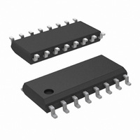
IC SW XPT 1.5GPS 2X2 LVDS 16SOIC
Manufacturer
National Semiconductor
Datasheet
1.DS10CP152TMANOPB.pdf
(12 pages)
Specifications of DS10CP152TMA/NOPB
Function
Crosspoint Switch
Circuit
1 x 2:2
Voltage Supply Source
Single Supply
Voltage - Supply, Single/dual (±)
3 V ~ 3.6 V
Current - Supply
58mA
Operating Temperature
-40°C ~ 85°C
Mounting Type
Surface Mount
Package / Case
16-SOIC (0.154", 3.90mm Width)
Supply Voltage Range
3V To 3.6V
Digital Ic Case Style
SOIC
No. Of Pins
16
Operating Temperature Range
-40°C To +85°C
Svhc
No SVHC (15-Dec-2010)
Base Number
10
Data Rate
1.5Gbps
Interface
LVDS
Rohs Compliant
Yes
Lead Free Status / RoHS Status
Lead free / RoHS Compliant
Other names
DS10CP152TMA
Available stocks
Company
Part Number
Manufacturer
Quantity
Price
Company:

Part Number:
DS10CP152TMA/NOPB
Manufacturer:
National Semiconductor
Quantity:
135


LVCMOS DC SPECIFICATIONS
V
V
I
I
V
LVDS INPUT DC SPECIFICATIONS
V
V
V
V
I
C
R
Symbol
IH
IL
IN
Supply Voltage
LVCMOS Input Voltage
LVDS Input Voltage
LVDS Differential Input Voltage
LVDS Output Voltage
LVDS Differential Output Voltage
LVDS Output Short Circuit Current
Duration
Junction Temperature
Storage Temperature Range
Lead Temperature Range
Maximum Package Power Dissipation at 25°C
IH
IL
CL
ID
TH
TL
CMR
IN
IN
Absolute Maximum Ratings
If Military/Aerospace specified devices are required,
please contact the National Semiconductor Sales Office/
Distributors for availability and specifications.
DC Electrical Characteristics
Over recommended operating supply and temperature ranges unless otherwise specified. (Notes 5, 6, 7)
Soldering (4 sec.)
M16A Package
Derate M16A Package
High Level Input Voltage
Low Level Input Voltage
High Level Input Current
Low Level Input Current
Input Clamp Voltage
Input Differential Voltage
Differential Input High Threshold
Differential Input Low Threshold
Common Mode Voltage Range
Input Current
Input Capacitance
Input Termination Resistor
Parameter
13.75 mW/°C above +25°C
−0.3V to (V
−0.3V to (V
−65°C to +150°C
(Note 4)
−0.3V to +4V
−0.3V to +4V
CC
CC
0V to 1V
0V to 1V
+150°C
+260°C
+ 0.3V)
+ 0.3V)
1.72W
5 ms
V
V
V
V
I
V
V
V
V
Any LVDS Input Pin to GND
Between IN+ and IN-
CL
IN
CC
IN
CC
CM
ID
IN
CC
= −18 mA, V
3
= 3.6V
= GND
= 100 mV
= 3.6V or 0V
= 3.6V
= 3.6V
= 3.6V or 0V
= +0.05V or V
Package Thermal Resistance
θ
θ
ESD Susceptibility
Note 1: Human Body Model, applicable std. JESD22-A114C
Note 2: Machine Model, applicable std. JESD22-A115-A
Note 3: Field Induced Charge Device Model, applicable std.
JESD22-C101-C
Recommended Operating
Conditions
Supply Voltage (V
Receiver Differential Input
Voltage (V
Operating Free Air
Temperature (T
HBM (Note 1)
MM (Note 2)
CDM (Note 3)
JA
JC
Conditions
CC
CC
= 0V
ID
-0.05V
)
A
)
CC
)
Min
−40
3.0
−100
GND
0.05
0
Min
2.0
40
0
Typ
+25
3.3
−0.9
Typ
175
100
1.7
±1
±1
0
0
Max
+85
3.6
1
V
+100
Max
−1.5
0.05
V
250
±10
±10
www.national.com
0.8
CC
1
DD
+72.7°C/W
+41.2°C/W
-
Units
≥
°C
≥
V
V
1250V
≥
Units
250V
7 kV
mV
mV
μA
μA
μA
pF
V
V
V
V
V
Ω
Related parts for DS10CP152TMA/NOPB
Image
Part Number
Description
Manufacturer
Datasheet
Request
R

Part Number:
Description:
National Semiconductor [8-Bit D/A Converter]
Manufacturer:
National Semiconductor
Datasheet:
Part Number:
Description:
National Semiconductor [Media Coprocessor]
Manufacturer:
National Semiconductor
Datasheet:
Part Number:
Description:
Digitally Controlled Tone and Volume Circuit with Stereo Audio Power Amplifier, Microphone Preamp Stage and National 3D Sound
Manufacturer:
National Semiconductor
Datasheet:
Part Number:
Description:
Digitally Controlled Tone and Volume Circuit with Stereo Audio Power Amplifier, Microphone Preamp Stage and National 3D Sound
Manufacturer:
National Semiconductor
Datasheet:
Part Number:
Description:
AC97 Rev 2 Codec with Sample Rate Conversion and National 3D Sound
Manufacturer:
National Semiconductor
Part Number:
Description:
Manufacturer:
National Semiconductor
Datasheet:
Part Number:
Description:
Manufacturer:
National Semiconductor
Datasheet:
Part Number:
Description:
General Purpose, Low Voltage, Low Power, Rail-to-Rail Output Operational Amplifiers
Manufacturer:
National Semiconductor
Datasheet:
Part Number:
Description:
8-bit 20 MSPS flash A/D converter.
Manufacturer:
National Semiconductor
Datasheet:
Part Number:
Description:
Low Noise Quad Operational Amplifier
Manufacturer:
National Semiconductor
Datasheet:
Part Number:
Description:
Quad Differential Line Receivers
Manufacturer:
National Semiconductor
Datasheet:
Part Number:
Description:
Quad High Speed Trapezoidal? Bus Transceiver
Manufacturer:
National Semiconductor
Datasheet:
Part Number:
Description:
Dual Line Receiver
Manufacturer:
National Semiconductor
Datasheet:
Part Number:
Description:
TTL to 10k ECL Level Translator with Latch
Manufacturer:
National Semiconductor
Datasheet: