DG413DJZ Intersil, DG413DJZ Datasheet - Page 2
DG413DJZ
Manufacturer Part Number
DG413DJZ
Description
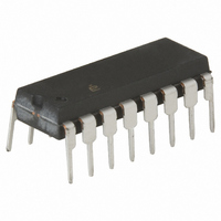
IC SWITCH QUAD SPST 16DIP
Manufacturer
Intersil
Type
Analog Switchr
Datasheet
1.DG411DYZ.pdf
(13 pages)
Specifications of DG413DJZ
Function
Switch
Circuit
4 x SPST - NC/NO
On-state Resistance
35 Ohm
Voltage Supply Source
Single, Dual Supply
Voltage - Supply, Single/dual (±)
5 V ~ 44 V, ±5 V ~ 20 V
Operating Temperature
-40°C ~ 85°C
Mounting Type
Through Hole
Package / Case
16-DIP (0.300", 7.62mm)
Package
16PDIP
Maximum On Resistance
80@10.8V Ohm
Maximum High Level Output Current
30 mA
Maximum Turn-off Time
145@±15V ns
Maximum Turn-on Time
250@12V ns
Switch Architecture
SPST
Power Supply Type
Single|Dual
Lead Free Status / RoHS Status
Lead free / RoHS Compliant
Available stocks
Company
Part Number
Manufacturer
Quantity
Price
Company:

Part Number:
DG413DJZ
Manufacturer:
Vishay
Quantity:
709


Ordering Information
NOTE: Logic “0” ≤0.8V. Logic “1” ≥2.4V.
Pinout
DG411DJ
DG411DJZ (Note)
DG411DY*
DG411DYZ* (Note)
DG411DVZ* (Note)
DG412DJ
DG412DJZ (Note)
DG412DY*
DG412DYZ* (Note)
DG412DVZ* (Note)
DG413DJ
DG413DJZ (Note)
DG413DY*
DG413DYZ* (Note)
DG413DVZ* (Note)
*Add “-T” suffix for tape and reel.
**Pb-free PDIPs can be used for through hole wave solder processing only. They are not intended for use in Reflow solder processing
applications.
NOTE: Intersil Pb-free plus anneal products employ special Pb-free material sets; molding compounds/die attach materials and 100% matte tin
plate termination finish, which are RoHS compliant and compatible with both SnPb and Pb-free soldering operations. Intersil Pb-free products
are MSL classified at Pb-free peak reflow temperatures that meet or exceed the Pb-free requirements of IPC/JEDEC J STD-020.
LOGIC
0
1
PART NUMBER
SWITCH SWITCH
DG411
On
Off
GND
(16 LD PDIP, SOIC, TSSOP)
IN
IN
D
S
S
D
V-
1
1
1
4
4
4
DG411, DG412, DG413
DG412
1
2
3
4
5
6
7
8
Off
On
TRUTH TABLE
TOP VIEW
DG411DJ
DG411DJZ
DG411DY
DG411DYZ
DG411 DVZ
DG412DJ
DG412DJZ
DG412DY
DG412DYZ
DG412 DVZ
DG413DJ
DG413DJZ
DG413DY
DG413DYZ
DG413 DVZ
2
SWITCH
PART MARKING
1, 4
On
Off
16
15
14
13
12
11
10
9
IN
D
S
V+
V
S
D
IN
DG413
2
L
3
2
3
2
3
SWITCH
DG411, DG412, DG413
2, 3
On
Off
TEMP. RANGE (°C)
-40 to +85
-40 to +85
-40 to +85
-40 to +85
-40 to +85
-40 to +85
-40 to +85
-40 to +85
-40 to +85
-40 to +85
-40 to +85
-40 to +85
-40 to +85
-40 to +85
-40 to +85
Pin Descriptions
PIN
10
11
12
13
14
15
16
1
2
3
4
5
6
7
8
9
SYMBOL
GND
IN
IN
IN
IN
D
S
S
D
D
S
V
V+
S
D
V-
1
4
3
L
2
1
4
3
2
1
4
3
2
16 Ld PDIP
16 Ld PDIP** (Pb-free)
16 Ld SOIC (150 mil)
16 Ld SOIC (150 mil) (Pb-free)
16 Ld TSSOP (4.4mm) (Pb-free) M16.173
16 Ld PDIP
16 Ld PDIP** (Pb-free)
16 Ld SOIC (150 mil)
16 Ld SOIC (150 mil) (Pb-free)
16 Ld TSSOP (4.4mm) (Pb-free) M16.173
16 Ld PDIP
16 Ld PDIP** (Pb-free)
16 Ld SOIC (150 mil)
16 Ld SOIC (150 mil) (Pb-free)
16 Ld TSSOP (4.4mm) (Pb-free) M16.173
Logic Control for Switch 1.
Drain (Output) Terminal for Switch 1.
Source (Input) Terminal for Switch 1.
Negative Power Supply Terminal.
Ground Terminal (Logic Common).
Source (Input) Terminal for Switch 4.
Drain (Output) Terminal for Switch 4.
Logic Control for Switch 4.
Logic Control for Switch 3.
Drain (Output) Terminal for Switch 3.
Source (Input) Terminal for Switch 3.
Logic Reference Voltage.
Positive Power Supply Terminal (Substrate).
Source (Input) Terminal for Switch 2.
Drain (Output) Terminal for Switch 2.
Logic Control for Switch 2.
PACKAGE
DESCRIPTION
E16.3
E16.3
M16.15
M16.15
E16.3
E16.3
M16.15
M16.15
E16.3
E16.3
M16.15
M16.15
PKG. DWG. #
June 20, 2007
FN3282.13
Related parts for DG413DJZ
Image
Part Number
Description
Manufacturer
Datasheet
Request
R

Part Number:
Description:
Intersil Corporation [CMOS Serial Controller Interface]
Manufacturer:
Intersil Corporation
Datasheet:
Part Number:
Description:
Manufacturer:
Intersil Corporation
Datasheet:
Part Number:
Description:
357-036-542-201 CARDEDGE 36POS DL .156 BLK LOPRO
Manufacturer:
Intersil Corporation
Datasheet:
Part Number:
Description:
1024-Word x 4-Bit LSI Static RAM
Manufacturer:
Intersil Corporation
Datasheet:
Part Number:
Description:
General Purpose NPN Transistor Arrays FN341.4
Manufacturer:
Intersil Corporation
Datasheet:
Part Number:
Description:
CMOS 16-Bit Microprocessor
Manufacturer:
Intersil Corporation
Datasheet:
Part Number:
Description:
Manufacturer:
Intersil Corporation
Datasheet:
Part Number:
Description:
Manufacturer:
Intersil Corporation
Datasheet:
Part Number:
Description:
Manufacturer:
Intersil Corporation
Datasheet:
Part Number:
Description:
Manufacturer:
Intersil Corporation
Datasheet:
Part Number:
Description:
CMOS 6-Bit Latch and Decoder Memory Interfaces
Manufacturer:
Intersil Corporation
Datasheet:
Part Number:
Description:
CA3046General Purpose NPN Transistor Arrays
Manufacturer:
Intersil Corporation
Datasheet:
Part Number:
Description:
Manufacturer:
Intersil Corporation
Datasheet:
Part Number:
Description:
TR909 DLC/FLC SLIC with Low Power Standby
Manufacturer:
Intersil Corporation
Datasheet:
Part Number:
Description:
Manufacturer:
Intersil Corporation
Datasheet: