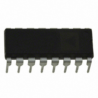
ADG508FBNZ Analog Devices Inc, ADG508FBNZ Datasheet - Page 10

ADG508FBNZ
Manufacturer Part Number
ADG508FBNZ
Description
IC MULTIPLEXER 8X1 16DIP
Manufacturer
Analog Devices Inc
Type
Analog Multiplexerr
Specifications of ADG508FBNZ
Function
Multiplexer
Circuit
1 x 8:1
On-state Resistance
300 Ohm
Voltage Supply Source
Dual Supply
Voltage - Supply, Single/dual (±)
±10.8 V ~ 16.5 V
Current - Supply
20µA
Operating Temperature
-40°C ~ 85°C
Mounting Type
Through Hole
Package / Case
16-DIP (0.300", 7.62mm)
No. Of Circuits
1
Supply Current
600µA
On State Resistance Max
300ohm
Supply Voltage Range
10.8V To 16.5V
Operating Temperature Range
-40°C To +85°C
Analog Switch Case Style
DIP
Multiplexer Configuration
Single 8:1
Number Of Inputs
8
Number Of Outputs
1
Number Of Channels
1
Analog Switch On Resistance
350@±15VOhm
Analog Switch Turn On Time
250ns
Analog Switch Turn Off Time
250ns
Package Type
PDIP
Power Supply Requirement
Dual
Single Supply Voltage (min)
Not RequiredV
Single Supply Voltage (typ)
Not RequiredV
Single Supply Voltage (max)
Not RequiredV
Dual Supply Voltage (typ)
±15V
Dual Supply Voltage (max)
±22V
Power Dissipation
3.3mW
Mounting
Through Hole
Pin Count
16
Operating Temp Range
-40C to 85C
Operating Temperature Classification
Industrial
Lead Free Status / RoHS Status
Lead free / RoHS Compliant
Lead Free Status / RoHS Status
Lead free / RoHS Compliant, Lead free / RoHS Compliant
ADG508F/ADG509F/ADG528F
TERMINOLOGY
V
Most Positive Power Supply Potential.
V
Most Negative Power Supply Potential.
GND
Ground (0 V) Reference.
R
Ohmic Resistance between D and S.
R
Change in R
Celsius.
R
Difference between the R
I
Source leakage current when the switch is off.
I
Drain leakage current when the switch is off.
I
Channel leakage current when the switch is on.
V
Analog Voltage on Terminals D, S.
C
Channel input capacitance for off condition.
C
Channel output capacitance for off condition.
C
On Switch Capacitance.
C
Digital Input Capacitance.
S
D
D
ON
ON
ON
S
D
D
IN
DD
SS
D
, I
(OFF)
(OFF)
, C
(OFF)
(V
(OFF)
S
Drift
Match
(ON)
S
S
)
(ON)
ON
when temperature changes by one degree
ON
of any two channels.
Rev. E | Page 10 of 20
t
Delay time between the 50% and 90% points of the digital input
and switch on condition.
t
Delay time between the 50% and 90% points of the digital input
and switch off condition.
t
Delay time between the 50% and 90% points of the digital
inputs and the switch on condition when switching from one
address state to another.
t
“OFF” time measured between 80% points of both switches
when switching from one address state to another.
V
Maximum input voltage for Logic 0.
V
Minimum input voltage for Logic 1.
I
Input current of the digital input.
Off Isolation
A measure of unwanted signal coupling through an off channel.
Charge Injection
A measure of the glitch impulse transferred from the digital
input to the analog output during switching.
I
Positive Supply Current.
I
Negative Supply Current.
ON
OFF
TRANSITION
OPEN
INL
DD
SS
INL
INH
(EN)
(I
(EN)
INH
)


