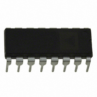
ADG508FBNZ Analog Devices Inc, ADG508FBNZ Datasheet - Page 7

ADG508FBNZ
Manufacturer Part Number
ADG508FBNZ
Description
IC MULTIPLEXER 8X1 16DIP
Manufacturer
Analog Devices Inc
Type
Analog Multiplexerr
Specifications of ADG508FBNZ
Function
Multiplexer
Circuit
1 x 8:1
On-state Resistance
300 Ohm
Voltage Supply Source
Dual Supply
Voltage - Supply, Single/dual (±)
±10.8 V ~ 16.5 V
Current - Supply
20µA
Operating Temperature
-40°C ~ 85°C
Mounting Type
Through Hole
Package / Case
16-DIP (0.300", 7.62mm)
No. Of Circuits
1
Supply Current
600µA
On State Resistance Max
300ohm
Supply Voltage Range
10.8V To 16.5V
Operating Temperature Range
-40°C To +85°C
Analog Switch Case Style
DIP
Multiplexer Configuration
Single 8:1
Number Of Inputs
8
Number Of Outputs
1
Number Of Channels
1
Analog Switch On Resistance
350@±15VOhm
Analog Switch Turn On Time
250ns
Analog Switch Turn Off Time
250ns
Package Type
PDIP
Power Supply Requirement
Dual
Single Supply Voltage (min)
Not RequiredV
Single Supply Voltage (typ)
Not RequiredV
Single Supply Voltage (max)
Not RequiredV
Dual Supply Voltage (typ)
±15V
Dual Supply Voltage (max)
±22V
Power Dissipation
3.3mW
Mounting
Through Hole
Pin Count
16
Operating Temp Range
-40C to 85C
Operating Temperature Classification
Industrial
Lead Free Status / RoHS Status
Lead free / RoHS Compliant
Lead Free Status / RoHS Status
Lead free / RoHS Compliant, Lead free / RoHS Compliant
THEORY OF OPERATION
The ADG508F/ADG509F/ADG528F multiplexers are capable
of withstanding overvoltages from –40 V to +55 V, irrespective
of whether the power supplies are present or not. Each channel
of the multiplexer consists of an n-channel MOSFET, a p-
channel MOSFET and an n-channel MOSFET, connected in
series. When the analog input exceeds the power supplies, one
of the MOSFETs will switch off, limiting the current to sub-
microamp levels, thereby preventing the overvoltage from dam-
aging any circuitry following the multiplexer. Figure 12 illustrates
the channel architecture that enables these multiplexers to with-
stand continuous overvoltages.
When an analog input of V
the ADG508F/ADG509F/ADG528F, the multiplexer behaves
as a standard multiplexer, with specifications similar to a stan-
dard multiplexer, for example, the on-resistance is 400
mum. However, when an overvoltage is applied to the device,
one of the three MOSFETs will turn off.
Figures 12 to 15 show the conditions of the three MOSFETs for
the various overvoltage situations. When the analog input ap-
plied to an ON channel approaches the positive power supply
line, the n-channel MOSFET turns OFF since the voltage on
the analog input exceeds the difference between V
REV. C
Figure 12. +55 V Overvoltage Input to the ON Channel
Figure 13. –40 V Overvoltage on an OFF Channel with
Multiplexer Power ON
OVERVOLTAGE
OVERVOLTAGE
n-CHANNEL
n-CHANNEL
MOSFET IS
MOSFET IS
+55V
–40V
OFF
ON
V
V
SS
DD
SS
+ 3 V to V
Q1
Q1
V
V
SS
DD
DD
Q2
Q2
p-CHANNEL
MOSFET IS
– 1.5 V is applied to
OFF
Q3
Q3
DD
and the
maxi-
–7–
n-channel threshold voltage (V
tive than V
MOSFET will turn off since the analog input is more negative
than the difference between V
voltage (V
3 V, the analog input range to the multiplexer is limited to
–12 V to +13.5 V when a 15 V power supply is used.
When the power supplies are present but the channel is off,
again either the p-channel MOSFET or one of the n-channel
MOSFETs will turn off when an overvoltage occurs.
Finally, when the power supplies are off, the gate of each
MOSFET will be at ground. A negative overvoltage switches
on the first n-channel MOSFET but the bias produced by the
overvoltage causes the p-channel MOSFET to remain turned
off. With a positive overvoltage, the first MOSFET in the
series will remain off since the gate to source voltage applied to
this MOSFET is negative.
During fault conditions, the leakage current into and out of the
ADG508F/ADG509F/ADG528F is limited to a few microamps.
This protects the multiplexer and succeeding circuitry from over
stresses as well as protecting the signal sources which drive the
multiplexer. Also, the other channels of the multiplexer will be
undisturbed by the overvoltage and will continue to operate
normally.
Figure 14. +55 V Overvoltage with Power OFF
Figure 15. –40 V Overvoltage with Power OFF
TP
OVERVOLTAGE
OVERVOLTAGE
SS
). Since V
ADG508F/ADG509F/ADG528F
is applied to the multiplexer, the p-channel
n-CHANNEL
MOSFET IS
n-CHANNEL
MOSFET IS
+55V
–40V
OFF
ON
TN
is nominally 1.5 V and V
SS
TN
Q1
Q1
and the p-channel threshold
). When a voltage more nega-
p-CHANNEL
MOSFET IS
Q2
Q2
OFF
Q3
Q3
TP
is typically


