DG444DY-T1-E3 Vishay, DG444DY-T1-E3 Datasheet - Page 2
DG444DY-T1-E3
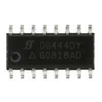
Manufacturer Part Number
DG444DY-T1-E3
Description
IC SWITCH QUAD SPST 16SOIC
Manufacturer
Vishay
Datasheet
1.DG444DY-T1-E3.pdf
(9 pages)
Specifications of DG444DY-T1-E3
Function
Switch
Circuit
4 x SPST - NC
On-state Resistance
85 Ohm
Current - Supply
5µA
Operating Temperature
-40°C ~ 85°C
Mounting Type
Surface Mount
Package / Case
16-SOIC (0.154", 3.90mm Width)
Number Of Switches
Quad
Switch Configuration
SPST
On Resistance (max)
160 Ohms
On Time (max)
450 ns
Off Time (max)
200 ns
Supply Voltage (max)
25 V
Supply Current
0.000001 mA
Maximum Power Dissipation
640 mW
Maximum Operating Temperature
+ 85 C
Mounting Style
SMD/SMT
Minimum Operating Temperature
- 40 C
Analog Switch Type
SPST
No. Of Channels
4
On State Resistance Max
50ohm
Turn Off Time
110ns
Turn On Time
120ns
Supply Voltage Range
10.8V To 13.2V
Lead Free Status / RoHS Status
Lead free / RoHS Compliant
Lead Free Status / RoHS Status
Lead free / RoHS Compliant, Lead free / RoHS Compliant
Other names
DG444DY-T1-E3TR
Available stocks
Company
Part Number
Manufacturer
Quantity
Price
Company:

Part Number:
DG444DY-T1-E3
Manufacturer:
AD
Quantity:
1 341
Part Number:
DG444DY-T1-E3
Manufacturer:
VISHAY/威世
Quantity:
20 000


DG444/445
Vishay Siliconix
V+ to V–
GND to V–
V
Digital Inputs
Continuous Current (Any Terminal)
Current, S or D (Pulsed 1 ms, 10% duty cycle)
Storage Temperature
www.vishay.com FaxBack 408-970-5600
4-2
Analog Switch
Analog Signal Range
Drain-Source On-Resistance
Switch Off Leakage Current
Switch Off Leakage Current
Channel On Leakage Current
Digital Control
Input Current V
Input Current V
Dynamic Characteristics
Turn-On Time
Turn-Off Time
Turn-Off Time
Charge Injection
Off Isolation
Crosstalk (Channel-to-Channel)
Source Off Capacitance
Drain Off Capacitance
Channel On Capacitance
Power Supplies
Positive Supply Current
Negative Supply Current
Logic Supply Current
Ground Current
L
. . . . . . . . . . . . . . . . . . . . . . . . . . . . . . . . . . . . . .
. . . . . . . . . . . . . . . . . . . . . . . . . . . . . . . . . . . . . . . . . . . . . . . . . . . . .
. . . . . . . . . . . . . . . . . . . . . . . . . . . . . . . . . . . . . . . . . . . . . . . . . . .
Parameter
a
e
V
S
IN
IN
, V
e
Low
High
D
d
. . . . . . . . . . . . . . . . . . . . . . . . . .
. . . . . . . . . . . . . . . . . . . . . . . . . . . . . . . . . .
d
. . . . . . . . . . . . . . . . . . . . . . . . . . . .
Symbol
V
or 30 mA, whichever occurs first
ANALOG
r
X
C
C
C
OIRR
DS(on)
I
I
I
I
t
t
S(off)
D(off)
D(on)
t
GND
OFF
OFF
TALK
D(off)
D(on)
S(off)
I
I
ON
. . . . . . . . . . . . . . . . . .
Q
I+
I–
(GND –0.3 V) to (V+) + 0.3 V
I
IL
IH
L
(V–) –2 V to (V+) +2 V
Unless Otherwise Specified
V
V
–65 to 125 C
S
S
R
R
R
R
=
L
L
V
V
L
L
V
I
= 1 k
= 1 k , C
S
D
V+ = 13.5 V, V– = –13.5 V
V+ = 16.5 V, V– = –16.5 V
V
V+ = 16.5 V, V– = –16.5 V
= 50
= 50
L
100 mA
V+ = 16.5, V– = –16.5 V
= –10 mA, V
10 V, See Figure 2
10 V, See Figure 2
=
V
V
30 mA
V+ = 15 V, V– = –15 V
Test Conditions
= 5 V, V
V
IN
C
gen
V
IN
44 V
25 V
All Other = 2.4 V
All Other = 0.8 V
S
L
16 5 V V
V
15 5 V V
15.5 V, V
under test = 2.4 V
V
V
under test = 0.8 V
= 1 nF, V
= V
ANALOG
= 0 V, R
C
, C
, C
IN
f = 1 MHz
f = 1 MHz
L
L
IN
D
= 0 or 5 V
L
L
,
= 35 pF
= 35 pF
= 5 pF, f = 1 MHz
= 5 pF, f = 1 MHz
,
0
=
= 2.4 V, 0.8 V
D
gen
S
= 0 V
S
=
15.5 V
5 V
=
= 0 V
Power Dissipation (Package)b
16-Pin Plastic DIP
16-Pin Narrow Body SOIC
Notes:
a.
b.
c.
d.
= 0
16 5 V
15 5 V
15.5 V
8.5 V
Signals on S
diodes. Limit forward diode current to maximum current ratings.
All leads welded or soldered to PC Board.
Derate 6 mW/ C above 75 C
Derate 8 mW/ C above 75 C
e
DG444
DG445
X
c
, D
. . . . . . . . . . . . . . . . . . . . . . . . . . . . . . . . . . . . . . . . .
X
Temp
, or IN
Room
Room
Room
Room
Room
Room
Room
Room
Room
Room
Room
Room
Room
Room
Room
Room
Room
Full
Full
Full
Full
Full
Full
Full
Full
Full
Full
Full
d
. . . . . . . . . . . . . . . . . . . . . . . . . . . . . . . . . .
X
a
exceeding V+ or V– will be clamped by internal
Min
–500
–500
–0.5
–0.5
–0.5
–15
–10
–5
–5
–1
–5
–1
–5
b
–40 to 85 C
D Suffix
–0.0001
–0.001
Typ
–0.01
0.001
0.001
0.01
120
110
160
100
50
–1
60
16
0.01
0.01
0.08
4
4
S-52433—Rev. F, 06-Sep-99
Document Number: 70054
c
Max
100
500
500
250
140
210
0.5
0.5
0.5
15
85
10
5
5
1
5
1
5
b
450 mW
640 mW
Unit
pC
nA
nA
nA
ns
dB
dB
pF
V
A
A
A
A
F
Related parts for DG444DY-T1-E3
Image
Part Number
Description
Manufacturer
Datasheet
Request
R

Part Number:
Description:
Analog Switch Quad SPST 16-Pin SOIC N
Manufacturer:
Vishay
Datasheet:

Part Number:
Description:
Analog Switch ICs SPST Analog Switch
Manufacturer:
Vishay
Datasheet:

Part Number:
Description:
Maxim's redesigned DG444/DG445 analog switches now feature on-resistance matching (4Ω max) between switches and guaranteed on-resistance flatness over the signal range (9Ω max)
Manufacturer:
Maxim
Datasheet:
Part Number:
Description:
357-036-542-201 CARDEDGE 36POS DL .156 BLK LOPRO
Manufacturer:
Vishay
Datasheet:
Part Number:
Description:
357-036-542-201 CARDEDGE 36POS DL .156 BLK LOPRO
Manufacturer:
Vishay
Datasheet:
Part Number:
Description:
357-036-542-201 CARDEDGE 36POS DL .156 BLK LOPRO
Manufacturer:
Vishay
Datasheet:
Part Number:
Description:
357-036-542-201 CARDEDGE 36POS DL .156 BLK LOPRO
Manufacturer:
Vishay
Datasheet:
Part Number:
Description:
357-036-542-201 CARDEDGE 36POS DL .156 BLK LOPRO
Manufacturer:
Vishay
Datasheet:
Part Number:
Description:
357-036-542-201 CARDEDGE 36POS DL .156 BLK LOPRO
Manufacturer:
Vishay
Datasheet:
Part Number:
Description:
357-036-542-201 CARDEDGE 36POS DL .156 BLK LOPRO
Manufacturer:
Vishay
Datasheet:
Part Number:
Description:
357-036-542-201 CARDEDGE 36POS DL .156 BLK LOPRO
Manufacturer:
Vishay
Datasheet:
Part Number:
Description:
357-036-542-201 CARDEDGE 36POS DL .156 BLK LOPRO
Manufacturer:
Vishay
Datasheet:
Part Number:
Description:
357-036-542-201 CARDEDGE 36POS DL .156 BLK LOPRO
Manufacturer:
Vishay
Datasheet:
Part Number:
Description:
357-036-542-201 CARDEDGE 36POS DL .156 BLK LOPRO
Manufacturer:
Vishay
Datasheet:
Part Number:
Description:
357-036-542-201 CARDEDGE 36POS DL .156 BLK LOPRO
Manufacturer:
Vishay
Datasheet: