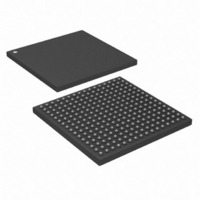
DS33X42+ Maxim Integrated Products, DS33X42+ Datasheet - Page 367

DS33X42+
Manufacturer Part Number
DS33X42+
Description
IC MAPPING ETHERNET 256CSBGA
Manufacturer
Maxim Integrated Products
Datasheet
1.DS33X11.pdf
(375 pages)
Specifications of DS33X42+
Applications
Data Transport
Interface
Parallel/Serial
Voltage - Supply
1.8V, 2.5V, 3.3V
Package / Case
256-CSBGA
Mounting Type
Surface Mount
Lead Free Status / RoHS Status
Lead free / RoHS Compliant
- Current page: 367 of 375
- Download datasheet (3Mb)
13.2 Instruction Register
The instruction register contains a shift register as well as a latched parallel output and is 3 bits in length. When the
TAP controller enters the Shift-IR state, the instruction shift register is connected between JTDI and JTDO. While in
the Shift-IR state, a rising edge on JTCLK with JTMS LOW will shift the data one stage towards the serial output at
JTDO. A rising edge on JTCLK in the Exit1-IR state or the Exit2-IR state with JTMS HIGH will move the controller
to the Update-IR state. The falling edge of that same JTCLK will latch the data in the instruction shift register to the
instruction parallel output. Instructions supported by the device and its respective operational binary codes are
shown in
Table 13-1. Instruction Codes for IEEE 1149.1 Architecture
13.2.1 SAMPLE:PRELOAD
This is a mandatory instruction for the IEEE 1149.1 specification. This instruction supports two functions. The
digital I/Os of the device can be sampled at the boundary scan register without interfering with the normal operation
of the device by using the Capture-DR state. SAMPLE:PRELOAD also allows the device to shift data into the
boundary scan register via JTDI using the Shift-DR state.
13.2.2 BYPASS
When the BYPASS instruction is latched into the parallel instruction register, JTDI connects to JTDO through the
one-bit bypass test register. This allows data to pass from JTDI to JTDO not affecting the device’s normal
operation.
13.2.3 EXTEST
This allows testing of all interconnections to the device. When the EXTEST instruction is latched in the instruction
register, the following actions occur. Once enabled via the Update-IR state, the parallel outputs of all digital output
pins are driven. The boundary scan register is connected between JTDI and JTDO. The Capture-DR will sample all
digital inputs into the boundary scan register.
13.2.4 CLAMP
All digital outputs of the device will output data from the boundary scan parallel output while connecting the bypass
register between JTDI and JTDO. The outputs will not change during the CLAMP instruction.
13.2.5 HIGHZ
All digital outputs of the device are placed in a high-impedance state. The BYPASS register is connected between
JTDI and JTDO.
13.2.6 IDCODE
When the IDCODE instruction is latched into the parallel instruction register, the identification test register is
selected. The device identification code is loaded into the identification register on the rising edge of JTCLK
following entry into the Capture-DR state. Shift-DR can be used to shift the identification code out serially via
JTDO. During Test-Logic-Reset, the identification code is forced into the instruction register’s parallel output. The
Rev: 063008
________________________________________________ DS33X162/X161/X82/X81/X42/X41/X11/W41/W11
SAMPLE:PRELOAD
INSTRUCTION
Table
BYPASS
EXTEST
IDCODE
CLAMP
HIGHZ
13-1.
SELECTED REGISTER
Device Identification
Boundary Scan
Boundary Scan
Bypass
Bypass
Bypass
INSTRUCTION CODES
010
111
000
011
100
001
367 of 375
Related parts for DS33X42+
Image
Part Number
Description
Manufacturer
Datasheet
Request
R

Part Number:
Description:
MAX7528KCWPMaxim Integrated Products [CMOS Dual 8-Bit Buffered Multiplying DACs]
Manufacturer:
Maxim Integrated Products
Datasheet:

Part Number:
Description:
Single +5V, fully integrated, 1.25Gbps laser diode driver.
Manufacturer:
Maxim Integrated Products
Datasheet:

Part Number:
Description:
Single +5V, fully integrated, 155Mbps laser diode driver.
Manufacturer:
Maxim Integrated Products
Datasheet:

Part Number:
Description:
VRD11/VRD10, K8 Rev F 2/3/4-Phase PWM Controllers with Integrated Dual MOSFET Drivers
Manufacturer:
Maxim Integrated Products
Datasheet:

Part Number:
Description:
Highly Integrated Level 2 SMBus Battery Chargers
Manufacturer:
Maxim Integrated Products
Datasheet:

Part Number:
Description:
Current Monitor and Accumulator with Integrated Sense Resistor; ; Temperature Range: -40°C to +85°C
Manufacturer:
Maxim Integrated Products

Part Number:
Description:
TSSOP 14/A�/RS-485 Transceivers with Integrated 100O/120O Termination Resis
Manufacturer:
Maxim Integrated Products

Part Number:
Description:
TSSOP 14/A�/RS-485 Transceivers with Integrated 100O/120O Termination Resis
Manufacturer:
Maxim Integrated Products

Part Number:
Description:
QFN 16/A�/AC-DC and DC-DC Peak-Current-Mode Converters with Integrated Step
Manufacturer:
Maxim Integrated Products

Part Number:
Description:
TDFN/A/65V, 1A, 600KHZ, SYNCHRONOUS STEP-DOWN REGULATOR WITH INTEGRATED SWI
Manufacturer:
Maxim Integrated Products

Part Number:
Description:
Integrated Temperature Controller f
Manufacturer:
Maxim Integrated Products

Part Number:
Description:
SOT23-6/I�/45MHz to 650MHz, Integrated IF VCOs with Differential Output
Manufacturer:
Maxim Integrated Products

Part Number:
Description:
SOT23-6/I�/45MHz to 650MHz, Integrated IF VCOs with Differential Output
Manufacturer:
Maxim Integrated Products

Part Number:
Description:
EVALUATION KIT/2.4GHZ TO 2.5GHZ 802.11G/B RF TRANSCEIVER WITH INTEGRATED PA
Manufacturer:
Maxim Integrated Products

Part Number:
Description:
QFN/E/DUAL PCIE/SATA HIGH SPEED SWITCH WITH INTEGRATED BIAS RESISTOR
Manufacturer:
Maxim Integrated Products
Datasheet:


