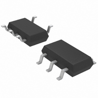
LTC1694CS5#TRPBF Linear Technology, LTC1694CS5#TRPBF Datasheet - Page 7

LTC1694CS5#TRPBF
Manufacturer Part Number
LTC1694CS5#TRPBF
Description
IC ACCEL SMBUS DUAL TSOT23-5
Manufacturer
Linear Technology
Datasheet
1.LTC1694CS5TRMPBF.pdf
(8 pages)
Specifications of LTC1694CS5#TRPBF
Applications
Data Transport
Interface
SMBus (2-Wire/I²C)
Voltage - Supply
2.7 V ~ 6 V
Package / Case
TSOT-23-5, TSOT-5, TSOP-5
Mounting Type
Surface Mount
Lead Free Status / RoHS Status
Lead free / RoHS Compliant
Available stocks
Company
Part Number
Manufacturer
Quantity
Price
APPLICATIO S I FOR ATIO
PACKAGE DESCRIPTIO
ACK Data Setup Time
The data setup time requirement for ACK (acknowledge)
must be fulfilled if a high value of R
edge is accomplished by the SMBus host releasing the
SDA line (pulling high) at the end of the last bit sent and the
SMBus slave device pulling the SDA line low before the
rising edge of the ACK clock pulse.
The LTC1694 2.2mA boosted pull-up current is activated
when the SMBus host releases the SDA line, allowing the
voltage to rise above the LTC1694’s comparator threshold
of 0.65V. If an SMBus slave device has a high value of R
0.20 BSC
NOTE:
1. DIMENSIONS ARE IN MILLIMETERS
2. DRAWING NOT TO SCALE
3. DIMENSIONS ARE INCLUSIVE OF PLATING
4. DIMENSIONS ARE EXCLUSIVE OF MOLD FLASH AND METAL BURR
5. MOLD FLASH SHALL NOT EXCEED 0.254mm
6. JEDEC PACKAGE REFERENCE IS MO-193
3.85 MAX
DATUM ‘A’
2.62 REF
U
RECOMMENDED SOLDER PAD LAYOUT
MAX
0.62
U
0.30 – 0.50 REF
PER IPC CALCULATOR
Information furnished by Linear Technology Corporation is believed to be accurate and reliable.
However, no responsibility is assumed for its use. Linear Technology Corporation makes no represen-
tation that the interconnection of its circuits as described herein will not infringe on existing patent rights.
S
W
0.95
is used. An acknowl-
REF
U
1.22 REF
1.4 MIN
(Reference LTC DWG # 05-08-1635)
0.09 – 0.20
(NOTE 3)
U
5-Lead Plastic TSOT-23
2.80 BSC
S5 Package
S
,
1.00 MAX
1.50 – 1.75
a longer time is required for this SMBus slave device to pull
SDA low before the rising edge of the ACK clock pulse.
To ensure sufficient data setup time for ACK, SMBus slave
devices, with high values of R
earlier. Typically, a minimum setup time of 1.5 s is needed
for an SMBus device with an R
capacitance of 200pF.
An alternative is that the SMBus slave device can hold SCL
line low until the SDA line reaches a stable state. Then, SCL
can be released to generate the ACK clock pulse.
(NOTE 4)
0.80 – 0.90
PIN ONE
0.95 BSC
2.90 BSC
(NOTE 4)
1.90 BSC
S
, should pull the SDA low
S
of 700
S5 TSOT-23 0302
0.30 – 0.45 TYP
5 PLCS (NOTE 3)
0.01 – 0.10
LTC1694
and a bus
1694fa
7


