FT245RL R FTDI, Future Technology Devices International Ltd, FT245RL R Datasheet - Page 35
FT245RL R
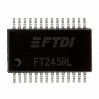
Manufacturer Part Number
FT245RL R
Description
IC USB TO PARALLEL FIFO 28-SSOP
Manufacturer
FTDI, Future Technology Devices International Ltd
Datasheet
1.FT245RL_R.pdf
(37 pages)
Specifications of FT245RL R
Applications
USB
Interface
USB
Voltage - Supply
1.8 V ~ 5.25 V
Package / Case
28-SSOP
Mounting Type
Surface Mount
For Use With
768-1020 - MODULE USB-PAR FIFO TTL 24-DIP
Lead Free Status / RoHS Status
Lead free / RoHS Compliant
Other names
768-1011-2
FT245RL R
FT245RL R


Document No.: FT_000052
FT245R USB FIFO IC Datasheet Version 2.10
Clearance No.: FTDI# 39
Appendix B - List of Figures and Tables
List of Figures
Figure 2.1 FT245R Block Diagram ................................................................................................... 4
Figure 3.1 SSOP Package Pin Out and Schematic Symbol ................................................................... 7
Figure 3.2 QFN-32 Package Pin Out and schematic symbol .............................................................. 10
Figure 3.3 FIFO Read Cycle .......................................................................................................... 13
Figure 3.4 FIFO Write Cycle ......................................................................................................... 14
Figure 6.1 Bus Powered Configuration ........................................................................................... 22
Figure 6.2 Self Powered Configuration ........................................................................................... 23
Figure 6.3 Bus Powered with Power Switching Configuration ............................................................ 24
Figure 6.4 USB Bus Powered with +3.3V or +5V External Logic Power Supply .................................... 25
Figure 7.1 USB to MCU FIFO Interface ........................................................................................... 26
Figure 9.1 SSOP-28 Package Dimensions ....................................................................................... 29
Figure 9.2 QFN-32 Package Dimensions ......................................................................................... 30
Figure 9.3 Typical Pad Layout for QFN-32 Package .......................................................................... 31
Figure 9.4 Typical Solder Paste Diagram for QFN-32 Package ........................................................... 31
Figure 9.5 FT245R Solder Reflow Profile ........................................................................................ 32
List of Tables
Table 3.1 USB Interface Group ....................................................................................................... 7
Table 3.2 Power and Ground Group ................................................................................................. 8
Table 3.3 Miscellaneous Signal Group .............................................................................................. 8
Table 3.4 FIFO Interface Group (see note 3) .................................................................................... 9
Table 3.5 USB Interface Group ..................................................................................................... 10
Table 3.6 Power and Ground Group ............................................................................................... 11
Table 3.7 Miscellaneous Signal Group ............................................................................................ 11
Table 3.8 FIFO Interface Group (see note 3) .................................................................................. 12
Table 3.9 FIFO Read Cycle Timings ............................................................................................... 13
Table 3.10 FIFO Write Cycle ......................................................................................................... 14
Table 5.1 Absolute Maximum Ratings ............................................................................................ 17
Table 5.2 Operating Voltage and Current ....................................................................................... 18
Table 5.3 FIFO I/O Pin Characteristics (VCCIO = +5.0V, Standard Drive Level) .................................. 18
Table 5.4 FIFO I/O Pin Characteristics (VCCIO = +3.3V, Standard Drive Level) .................................. 18
Table 5.5 FIFO I/O Pin Characteristics (VCCIO = +2.8V, Standard Drive Level) .................................. 19
Table 5.6 FIFO I/O Pin Characteristics (VCCIO = +1.8V, Standard Drive Level) .................................. 19
Table 5.7 FIFO I/O Pin Characteristics (VCCIO = +5.0V, High Drive Level) ......................................... 19
Table 5.8 FIFO I/O Pin Characteristics (VCCIO = +3.3V, High Drive Level) ......................................... 19
Table 5.9 FIFO I/O Pin Characteristics (VCCIO = +2.8V, High Drive Level) ......................................... 20
Table 5.10 FIFO I/O Pin Characteristics (VCCIO = +1.8V, High Drive Level) ....................................... 20
Copyright © 2010 Future Technology Devices International Limited
35
Related parts for FT245RL R
Image
Part Number
Description
Manufacturer
Datasheet
Request
R

Part Number:
Description:
IC USB TO SERIAL UART 32-QFN
Manufacturer:
FTDI, Future Technology Devices International Ltd

Part Number:
Description:
IC USB HOST CTLR VINCULUM 48LQFP
Manufacturer:
FTDI, Future Technology Devices International Ltd
Datasheet:

Part Number:
Description:
IC USB HOST VINCULUM-II 32QFN
Manufacturer:
FTDI, Future Technology Devices International Ltd
Datasheet:
Part Number:
Description:
IC USB HOST VINCULUM-II 32LQFN
Manufacturer:
FTDI, Future Technology Devices International Ltd
Datasheet:
Part Number:
Description:
IC USB HOST VINCULUM-II 48QFN
Manufacturer:
FTDI, Future Technology Devices International Ltd
Datasheet:
Part Number:
Description:
IC USB HOST VINCULUM-II 32LQFN
Manufacturer:
FTDI, Future Technology Devices International Ltd
Datasheet:
Part Number:
Description:
IC USB HOST VINCULUM-II 32QFN
Manufacturer:
FTDI, Future Technology Devices International Ltd
Datasheet:
Part Number:
Description:
IC USB HOST VINCULUM-II 48LQFP
Manufacturer:
FTDI, Future Technology Devices International Ltd
Datasheet:
Part Number:
Description:
IC USB HOST VINCULUM-II 48LQFP
Manufacturer:
FTDI, Future Technology Devices International Ltd
Datasheet:
Part Number:
Description:
IC USB HOST VINCULUM-II 48QFN
Manufacturer:
FTDI, Future Technology Devices International Ltd
Datasheet:
Part Number:
Description:
IC USB HOST CTLR VINCULUM 64QFN
Manufacturer:
FTDI, Future Technology Devices International Ltd
Datasheet:

Part Number:
Description:
IC USB HOST CTLR VINCULUM 64LQFP
Manufacturer:
FTDI, Future Technology Devices International Ltd
Datasheet:
Part Number:
Description:
IC USB HOST VINCULUM-II 64LQFP
Manufacturer:
FTDI, Future Technology Devices International Ltd
Datasheet:
Part Number:
Description:
IC USB HOST VINCULUM-II 64QFN
Manufacturer:
FTDI, Future Technology Devices International Ltd
Datasheet:

Part Number:
Description:
IC USB TO PARALLEL FIFO 32-QFN
Manufacturer:
FTDI, Future Technology Devices International Ltd
Datasheet: