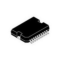
NCV7729BPPR2G ON Semiconductor, NCV7729BPPR2G Datasheet - Page 15

NCV7729BPPR2G
Manufacturer Part Number
NCV7729BPPR2G
Description
IC DRIVER H-BRIDGE 8A 20PSOP
Manufacturer
ON Semiconductor
Series
-r
Datasheet
1.NCV7729BPPR2G.pdf
(26 pages)
Specifications of NCV7729BPPR2G
Applications
DC Motor Driver, Stepper Motor Driver, H Bridge
Evaluation Tools
*
Number Of Outputs
1
Current - Output
5A
Voltage - Load
5 V ~ 28 V
Voltage - Supply
3 V ~ 5.5 V
Operating Temperature
-40°C ~ 150°C
Mounting Type
*
Package / Case
*
Motor Type
Half Bridge
No. Of Outputs
1
Output Current
9.6A
Supply Voltage Range
5V To 28V
Driver Case Style
SOP
No. Of Pins
20
Operating Temperature Range
-40°C To +150°C
Svhc
No SVHC
Rohs Compliant
Yes
Lead Free Status / Rohs Status
Compliant
Available stocks
Company
Part Number
Manufacturer
Quantity
Price
Company:
Part Number:
NCV7729BPPR2G
Manufacturer:
ON Semiconductor
Quantity:
500
Part Number:
NCV7729BPPR2G
Manufacturer:
ON/安森美
Quantity:
20 000
overvoltage is handled as a latched lockout condition,
requiring re−enable of the device by appropriate transitions
on the EN and DIS/SF (Config.SFMODE = 0) enable inputs.
Diagnostic and status information is lost when V
overvoltage occurs and it is required to re−program the
configuration register unless default settings are used.
Loss of Ground Failure
potential (G
In the event of ground loss failure, the device transitions into
fault lockout state and the output stages are turned into Hi−Z
mode. Loss of ground is handled as a latched lockout
condition. Diagnostic and status information is lost when
loss of ground occurs.
Fault Handling
overcurrent and overtemperature events cause a latched
lockout of the output stages. V
or loss of AGND or DGND faults are handled as a latched
lockout condition, requiring re−enable of the device. The
device can be returned to normal operating mode by either
a rising edge on EN while DIS/SF = 0, or a falling edge on
DIS/SF while EN = 1. Undervoltage on V
a non−latched lockout event (OUTx = Z until the supply
voltage returns into operating range).
be set low when EN goes H→L and is reset when EN goes
L→H. The status flag is set and latched when a fault
condition is detected that causes transition to a latched
lockout state. In the case of V
status flag is set, but is reset when the supply voltage returns
into operating range (see Table 1).
Loss of ground failure is detected when a difference in
Fault handling states are shown in Figure 11. All
In status flag mode (Config.SFMODE = 1), DIS/SF will
DIF
) between the AGND and DGND pins exists.
OUTx controlled by:
EN, DIS/SF, INx,
SPI:Config. ENx
CC
S
or CHP undervoltage the
under/over voltage faults
Device enable:
DIS/SF: H → L
EN: L → H
Operation
Normal
V(CHP)−V(VS) < VCHPLY
Figure 11. Fault Handling State Diagram
S
V(VS) < VSPORoff
or CHP result in
(Shorted Load, Overcurrent,
Output Fault Condition
V(CHP)−V(VS) > VCHPLY
or
V(VCC) < VCCPORon
V(VS) > VSPORon
Overtemp)
V(VCC) > VCCOV
http://onsemi.com
AND
OR
CC
15
that lead to a fault lockout state are stored in the diagnostic
register in a latched manner. A fault lockout state also causes
the configuration register “LOCK” bit to be set
(RD_Config:b4 = 1). In the case of VS or CHP undervoltage
the configuration “LOCK” bit is not set and diagnostic
register data is not latched (see Note 18 on Page 20).
until the microcontroller performs an action to reset the
device or register. The device status can be read by accessing
the diagnostic register via the RD_Diag or WR_Config SPI
commands. The state of the “LOCK” bit can be accessed via
the RD_Config command.
The diagnostic register can be reset by:
•
•
•
command or disabling the outputs via the Config.ENx bits
does not reset the diagnostic register contents.
The configuration register “LOCK” bit can be reset by:
•
•
= 0xF0 and configuration register “LOCK” bit b4 = 1.
All fault conditions (except V
Diagnostic and configuration register data will persist
Accessing the diagnostic register via the WR_Config
At power−up, default diagnostic register content is b[7:0]
A read access to the register via SPI command
RD_Diag (reset occurs on the rising edge of CSB if
valid SPI frame)
A rising edge on EN while DIS/SF = 0 or a falling edge
on DIS/SF while EN = 1
VCC under/over voltage or loss of AGND or DGND
A rising edge on EN while DIS/SF = 0 or a falling edge
on DIS/SF while EN = 1
VCC under/over voltage or loss of AGND or DGND
VCCOV / VCCUV
Loss of AGND or
Undervoltage
VS / CHP
Lockout
DGND
Fault
Power−up
V(VCC) > VCCPORon
(if configured as output )
Default settings
(if configured as output )
SPI Reset –
DIS/SF = L
OUTx = Z
OUTx = Z
DIS/SF = L
OUTx = Z
CC
or loss of ground faults)


