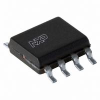
PCA9510AD,118 NXP Semiconductors, PCA9510AD,118 Datasheet - Page 13

PCA9510AD,118
Manufacturer Part Number
PCA9510AD,118
Description
IC I2C/SMBUS BUFF 8TSSOP
Manufacturer
NXP Semiconductors
Type
Bufferr
Datasheet
1.PCA9510ADP118.pdf
(24 pages)
Specifications of PCA9510AD,118
Package / Case
8-SOIC (3.9mm Width)
Tx/rx Type
I²C Logic
Delay Time
35ns
Capacitance - Input
1.9pF
Voltage - Supply
2.7 V ~ 5.5 V
Current - Supply
6mA
Mounting Type
Surface Mount
Logic Family
PCA
Supply Voltage (max)
7 V
Supply Voltage (min)
- 0.5 V
Maximum Operating Temperature
+ 85 C
Mounting Style
SMD/SMT
Minimum Operating Temperature
- 40 C
Output Voltage
0.3 V
Propagation Delay Time
80 ns
Supply Current
3.5 mA
Logic Type
SMBus Bus Buffer
Lead Free Status / RoHS Status
Lead free / RoHS Compliant
Lead Free Status / RoHS Status
Lead free / RoHS Compliant, Lead free / RoHS Compliant
Other names
935280025118
PCA9510AD-T
PCA9510AD-T
PCA9510AD-T
PCA9510AD-T
Available stocks
Company
Part Number
Manufacturer
Quantity
Price
Part Number:
PCA9510AD,118
Manufacturer:
NXP/恩智浦
Quantity:
20 000
NXP Semiconductors
Table 5.
V
[1]
[2]
[3]
[4]
[5]
[6]
[7]
PCA9510A_4
Product data sheet
Symbol
Input-output connection
V
t
t
C
V
I
System characteristics
f
t
t
t
t
t
t
t
t
t
t
PLH
PHL
LI
SCL
BUF
HD;STA
SU;STA
SU;STO
HD;DAT
SU;DAT
LOW
HIGH
f
r
CC
offset
OL
i(SCL/SDA)
= 2.7 V to 5.5 V; T
This specification applies over the full operating temperature range.
The enable time can slow considerably for some parts when temperature is < 20 C.
Delays that can occur after ENABLE and/or idle times have passed.
Guaranteed by design, not production tested.
The connection circuitry always regulates its output to a higher voltage than its input. The magnitude of this offset voltage as a function
of the pull-up resistor and V
Force V
output.
C
b
= total capacitance of one bus line in pF.
SDAIN
Characteristics
Parameter
offset voltage
LOW to HIGH
propagation delay
HIGH to LOW
propagation delay
SCL and SDA input
capacitance
LOW-level output voltage
input leakage current
SCL clock frequency
bus free time between a
STOP and START
condition
hold time (repeated)
START condition
set-up time for a repeated
START condition
set-up time for STOP
condition
data hold time
data set-up time
LOW period of the SCL
clock
HIGH period of the SCL
clock
fall time of both SDA and
SCL signals
rise time of both SDA and
SCL signals
= V
SCLIN
amb
= 0.1 V, tie SDAOUT and SCLOUT through 10 k resistor to V
= 40 C to +85 C; unless otherwise specified.
…continued
CC
voltage is shown in
Conditions
10 k to V
V
SCLn to SCLn and
SDAn to SDAn; 10 k to V
C
SCLn to SCLn and
SDAn to SDAn; 10 k to V
C
V
I
SDAn, SCLn pins; V
sink
CC
I
L
L
= 0 V; SDAn, SCLn pins;
= 100 pF each side
= 100 pF each side
= 3 mA; V
= 3.3 V
Section 11.1 “Typical performance
Rev. 04 — 18 August 2009
CC
on SDA, SCL;
CC
= 2.7 V
CC
= 5.5 V
CC
CC
;
;
Hot swappable I
[1][5]
[4][7]
[4][7]
[6]
[4]
[1]
[4]
[4]
[4]
[4]
[4]
[4]
[4]
[4]
[4]
CC
characteristics”.
Min
0
-
-
-
0
0
1.3
0.6
0.6
0.6
300
100
1.3
0.6
20 + 0.1
20 + 0.1
1
and measure the SDAOUT and SCLOUT
2
C-bus and SMBus bus buffer
C
C
b
b
Typ
110
800
80
5
0.3
-
-
-
-
-
-
-
-
-
-
-
-
PCA9510A
© NXP B.V. 2009. All rights reserved.
Max
175
-
-
7
0.4
+1
400
-
-
-
-
-
-
-
-
300
300
13 of 24
Unit
mV
ns
ns
pF
V
kHz
ns
ns
ns
ns
A
s
s
s
s
s
s


