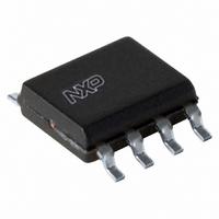
PCA9515D,118 NXP Semiconductors, PCA9515D,118 Datasheet - Page 5

PCA9515D,118
Manufacturer Part Number
PCA9515D,118
Description
IC I2C BUS REPEATER 8SOIC
Manufacturer
NXP Semiconductors
Type
Repeaterr
Datasheet
1.PCA9515DP118.pdf
(16 pages)
Specifications of PCA9515D,118
Tx/rx Type
I²C Logic
Delay Time
55ns
Capacitance - Input
6pF
Voltage - Supply
3 V ~ 3.6 V
Current - Supply
2.3mA
Mounting Type
Surface Mount
Package / Case
8-SOIC (3.9mm Width)
Lead Free Status / RoHS Status
Lead free / RoHS Compliant
Other names
935268651118
PCA9515D-T
PCA9515D-T
PCA9515D-T
PCA9515D-T
NXP Semiconductors
7. Application design-in information
PCA9515_9
Product data sheet
A typical application is shown in
on a 3.3 V I
unless the slave bus is isolated and then the master bus can run at 400 kHz. Master
devices can be placed on either bus.
The PCA9515 is 5 V tolerant so it does not require any additional circuitry to translate
between the different bus voltages.
When one side of the PCA9515 is pulled LOW by a device on the I
hysteresis type input detects the falling edge and causes an internal driver on the other
side to turn on, thus causing the other side to also go LOW. The side driven LOW by the
PCA9515 will typically be at V
In order to illustrate what would be seen in a typical application, refer to
Figure
would see the waveform shown in
transmission until the falling edge of the 8
the data line (SDA) while the slave pulls it LOW through the PCA9515. Because the V
the PCA9515 is typically around 0.5 V, a step in the SDA will be seen. After the master
has transmitted the 9
On the Bus 1 side of the PCA9515, the clock and data lines would have a positive offset
from ground equal to the V
be pulled to the V
It is important to note that any arbitration or clock stretching events on Bus 1 require that
the V
Section 9 “Static
to Bus 0.
Fig 4.
OL
6. If the bus master in
of the devices on Bus 1 be 70 mV below the V
Typical application
2
C-bus while the slave is connected to a 5 V bus. Both buses run at 100 kHz
characteristics”) to be recognized by the PCA9515 and then transmitted
OL
MASTER
400 kHz
BUS
of the slave device that is very close to ground in our example.
th
SDA
SCL
clock pulse, the slave releases the data line.
Rev. 09 — 23 April 2009
OL
bus 0
Figure 4
3.3 V
of the PCA9515. After the 8
OL
Figure
= 0.5 V.
Figure 5
SDA0
SCL0
EN
were to write to the slave through the PCA9515, we
4. In this example, the system master is running
V
CC
PCA9515
th
on Bus 0. This looks like a normal I
clock pulse. At that point, the master releases
SDA1
SCL1
OL
of the PCA9515 (see V
bus 1
th
5 V
clock pulse, the data line will
SDA
SCL
100 kHz
SLAVE
002aae621
2
C-bus, a CMOS
PCA9515
© NXP B.V. 2009. All rights reserved.
Figure 5
I
2
C-bus repeater
2
OL
C-bus
and
V
5 of 16
OL
ILc
of
in


