DS32EL0124SQ/NOPB National Semiconductor, DS32EL0124SQ/NOPB Datasheet - Page 11
DS32EL0124SQ/NOPB
Manufacturer Part Number
DS32EL0124SQ/NOPB
Description
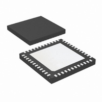
IC DESERIAL W/DDR LVDS 48LLP
Manufacturer
National Semiconductor
Datasheet
1.DS32EL0124SQENOPB.pdf
(28 pages)
Specifications of DS32EL0124SQ/NOPB
Function
Deserializer
Data Rate
3.125Gbps
Input Type
LVDS
Output Type
LVDS
Number Of Inputs
5
Number Of Outputs
1
Voltage - Supply
2.5V, 3.3V
Operating Temperature
-40°C ~ 85°C
Mounting Type
Surface Mount
Package / Case
48-LLP
Lead Free Status / RoHS Status
Lead free / RoHS Compliant
Other names
DS32EL0124SQ


Functional Description
POWER SUPPLIES
The DS32EL0124 and DS32ELX0124 have several power
supply pins, at 2.5V as well as 3.3V. It is important that these
pins all be connected and properly bypassed. Bypassing
should consist of parallel 4.7μF and 0.1μF capacitors as a
minimum, with a 0.1μF capacitor on each power pin. A 22 μF
capacitor is required on the VDDPLL pin which is connected
to the 3.3V rail.
These devices have a large contact in the center on the bot-
tom of the package. This contact must be connected to the
system GND as it is the major ground connection for the de-
vice.
POWER UP
It is recommended, although not necessary, to bring up the
3.3V power supply before the 2.5V supply. If the 2.5V supply
is powered up first, an initial current draw of approximately
600mA from the 2.5V rail may occur before settling to its final
value. Regardless of the sequence, both power rails should
monotonically ramp up to their final values.
POWER MANAGEMENT
These devices have two methods to reduce power consump-
tion. To enter the first power save mode, the on board host
FPGA or controlling device can cease to output the DDR
transmit clock. To further reduce power, a write to the power
down register will put the device in its lowest power mode.
RESET
There are three ways to reset these devices. A reset occurs
automatically during power-up. The device can also be reset
by pulling the RESET pin low, with normal operation resuming
when the pin is driven high again. The device can also be
reset by writing to the reset register. This reset will put all of
the register values back to their default values, except it will
not affect the address register value if the SMBus default ad-
dress has been changed.
LVDS OUTPUTS
The DS32EL0124 and DS32ELX0124 has standard LVDS
outputs, compatible with ANSI/TIA/EIA-644. It is recommend-
ed that the PCB trace between the FPGA and the deserializer
output be no more than 40-inches. Longer PCB traces may
introduce signal degradation as well as channel skew which
could cause serialization errors. The connection between the
host and the DS32EL0124 or DS32ELX0124 should be over
a controlled impedance transmission line with impedance that
matches the termination resistor – usually 100Ω. Setup and
hold times are specified in the LVDS Switching Characteris-
tics table, however the clock delay can be adjusted by writing
to register 30’h.
LOOP FILTER
The DS32EL0124 and DSELX0124 have an internal clock
data recovery module (CDR), which is used to recover the
input serial data. The loop filter for this CDR is external, and
for optimum results, a 30nF capacitor should be connected
between pins 26 and 27. See the Typical Interface Circuit
(Figure
12).
11
LOOP THROUGH DRIVER LAUNCH AMPLITUDE
The launch amplitude of the retimed CML loop through driver
is controlled by placing a single resistor from the VOD_CTRL
pin to ground. Use the following equation to obtain the desired
V
The retimed CML loop through driver launch amplitude can
also be adjusted by writing to SMBus register 49'h, bits 3:1.
This register is meant to assist system designers during the
initial prototype design phase. For final production, it is rec-
ommended that the appropriate resistor value be selected for
the desired V
value.
REMOTE SENSE
The remote sense feature can be used when a DS32EL0421
or DS32ELX0421 serializer is directly connected to a
DS32EL0124 or DS32ELX0124 deserializer. Active compo-
nents in the signal path between the serializer and the dese-
rializer may interfere with the back channel signaling of the
devices.
When remote sense is enabled, the deserializer will cycle
through five states to successfully establish a link and align
the data. The state diagram for the deserialiezr is shown in
Figure
state until it receives an input signal. Once the CDR of the
deserializer has locked to the input clock, the device will enter
the LINK DETECT state. While in this state, the deserializer
will monitor the line to see if the serializer is sending the train-
ing pattern. While in this state, the deserializer will periodically
send a link detect signal upstream to notify the serializer that
it can now send the training pattern. When the deserializer
detects that data coming in on the serial line, it will proceed
to the CLOCK ACQUISITION state. While in this state the
deserializer will monitor the incoming data for set periods of
time in an attempt to extract the clock from the data. Once,
the deserializer has successfully extracted the clock the de-
vice will proceed to the LINK ACQUISITION STATE. In this
state the deserializer will perform lane alignment based on the
expected training pattern and then enter the NORMAL state.
If the deserializer is unable to successfully lock or maintain
lock, it will break the link sending the serializer back to the
IDLE or LINK DETECT states.
DC-BALANCE DECODER
The DS32EL0124 and DS32ELX0124 have a built-in DC-bal-
ance decoder to support AC-coupled applications. When en-
abled, the output signal RxOUT4+/-, is treated as a data valid
bit. If RxOUT4+/- is low, then the data output from RxOUT0 -
RxOUT3 has been successfully decoded using the 8b/10b
coding scheme. If RxOUT4+/- is high and the outputs Rx-
OUT0 - RxOUT3 are high then an invalid 8b/10b code was
received, signifying a bit error. If RxOUT4+/- is high and the
outputs RxOUT0 - RxOUT3 are low then an idle character has
been received. The default idle character is a K28.5 code. In
order to properly receive other K codes, they must first be
programmed into the deserializer via the SMBus. The SMBus
registers allow for only a single programmable character.
LTOD
by selecting the corresponding resistor value.
7. The deserialzer will remain in the low power IDLE
LTOD
R = (1400 mV / V
and that register 49'h be left to its default
LTOD
) x 9.1 kΩ
www.national.com
Related parts for DS32EL0124SQ/NOPB
Image
Part Number
Description
Manufacturer
Datasheet
Request
R

Part Number:
Description:
National Semiconductor [8-Bit D/A Converter]
Manufacturer:
National Semiconductor
Datasheet:
Part Number:
Description:
National Semiconductor [Media Coprocessor]
Manufacturer:
National Semiconductor
Datasheet:
Part Number:
Description:
Digitally Controlled Tone and Volume Circuit with Stereo Audio Power Amplifier, Microphone Preamp Stage and National 3D Sound
Manufacturer:
National Semiconductor
Datasheet:
Part Number:
Description:
Digitally Controlled Tone and Volume Circuit with Stereo Audio Power Amplifier, Microphone Preamp Stage and National 3D Sound
Manufacturer:
National Semiconductor
Datasheet:
Part Number:
Description:
AC97 Rev 2 Codec with Sample Rate Conversion and National 3D Sound
Manufacturer:
National Semiconductor
Part Number:
Description:
Manufacturer:
National Semiconductor
Datasheet:
Part Number:
Description:
Manufacturer:
National Semiconductor
Datasheet:
Part Number:
Description:
General Purpose, Low Voltage, Low Power, Rail-to-Rail Output Operational Amplifiers
Manufacturer:
National Semiconductor
Datasheet:
Part Number:
Description:
8-bit 20 MSPS flash A/D converter.
Manufacturer:
National Semiconductor
Datasheet:
Part Number:
Description:
Low Noise Quad Operational Amplifier
Manufacturer:
National Semiconductor
Datasheet:
Part Number:
Description:
Quad Differential Line Receivers
Manufacturer:
National Semiconductor
Datasheet:
Part Number:
Description:
Quad High Speed Trapezoidal? Bus Transceiver
Manufacturer:
National Semiconductor
Datasheet:
Part Number:
Description:
Dual Line Receiver
Manufacturer:
National Semiconductor
Datasheet:
Part Number:
Description:
TTL to 10k ECL Level Translator with Latch
Manufacturer:
National Semiconductor
Datasheet: