DS92LV1212TMSA National Semiconductor, DS92LV1212TMSA Datasheet - Page 6
DS92LV1212TMSA
Manufacturer Part Number
DS92LV1212TMSA
Description
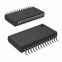
IC DESERIALZR RANDOM LOCK 28SSOP
Manufacturer
National Semiconductor
Datasheet
1.DS92LV1212TMSA.pdf
(13 pages)
Specifications of DS92LV1212TMSA
Function
Deserializer
Data Rate
400Mbps
Input Type
LVDS
Output Type
LVDS
Number Of Inputs
1
Number Of Outputs
10
Voltage - Supply
3 V ~ 3.6 V
Operating Temperature
-40°C ~ 85°C
Mounting Type
Surface Mount
Package / Case
28-SSOP
Lead Free Status / RoHS Status
Lead free / RoHS Compliant
Other names
*DS92LV1212TMSA
Available stocks
Company
Part Number
Manufacturer
Quantity
Price

Part Number:
DS92LV1212TMSA
Manufacturer:
NS/国半
Quantity:
20 000
Part Number:
DS92LV1212TMSAX
Manufacturer:
NS/国半
Quantity:
20 000
Company:
Part Number:
DS92LV1212TMSAX/NOPB
Manufacturer:
NS
Quantity:
7 081


www.national.com
Symbol
t
t
t
t
t
t
t
t
t
t
t
t
t
t
t
RCP
CLH
CHL
DD
ROS
ROH
RDC
HZR
LZR
ZHR
ZLR
DSR1
DSR2
ZHLK
RNM
Over recommended operating supply and temperature ranges unless otherwise specified.
Deserializer Switching Characteristics
Note 1: “Absolute Maximum Ratings” are those values beyond which the safety of the device cannot be guaranteed. They are not meant to imply that the devices
should be operated at these limits. The table of “Electrical Characteristics” specifies conditions of device operation.
Note 2: Typical values are given for V
Note 3: Current into device pins is defined as positive. Current out of device pins is defined as negative. Voltages are referenced to ground except VOD, VOD, VTH
and VTL which are differential voltages.
Note 4: For the purpose of specifying Deserializer PLL performance tDSR1 and tDSR2 are specified with the REFCLK running and stable, and specific conditions
of the incoming data stream (SYNCPATs). It is recommended that the Deserializer be initialized using either tDSR1 timing or tDSR2 timing. tDSR1 is the time required
for the Deserializer to indicate lock upon power-up or when leaving the power-down mode. Synchronization patterns should be sent to the device before initiating ei-
ther condition. tDSR2 is the time required to indicate lock for the powered-up and enabled Deserializer when the input (RI+ and RI-) conditions change from not re-
ceiving data to receiving synchronization patterns (SYNCPATs).
Note 5: tRNM is a measure of how much phase noise (jitter) the Deserializer can tolerate in the incoming data stream before bit errors occur.
Receiver out Clock
Period
CMOS/TTL Low-to-High
Transition Time
CMOS/TTL High-to-Low
Transition Time
Deserializer Delay
ROUT (0-9) Setup Data to
RCLK
ROUT (0-9) Hold Data to
RCLK
RCLK Duty Cycle
HIGH to TRI-STATE Delay
LOW to TRI-STATE Delay
TRI-STATE to HIGH Delay
TRI-STATE to LOW Delay
Deserializer PLL Lock Time
from PWRDWN (with
SYNCPAT)
Deserializer PLL Lock time
from SYNCPAT
TRI-STATE to HIGH Delay
(power-up)
Deserializer Noise Margin
Parameter
CC
= 3.3V and T
Figure 3
t
CL = 15 pF
Figure 2
Figure 4
Figure 5
Figure 6
(Note 4)
Figure 7
Figure 8
Figure 9
(Note 5)
RCP
Conditions
A
= t
= +25˚C.
TCP
LOCK, RCLK
16MHz
40MHz
16MHz
40MHz
16 MHz
40 MHz
Rout(0-9),
Rout(0-9),
Pin/Freq.
RCLK
RCLK
LOCK
LOCK
6
1.75*t
−0.4*t
0.4*t
Min
400
100
RCP
RCP
25
40
RCP
+ 1.5
1.75*t
4.2+0.5*t
4.5+0.5*t
6.0+0.5*t
6+0.5*t
−0.5*t
0.5*t
1100
18.2
21.0
14.4
4.62
Typ
400
7.4
50
RCP
2
2
RCP
RCP
RCP
+4.0
RCP
RCP
RCP
1.75*t
10+t
10+t
12+t
12+t
Max
62.5
25.6
60
22
30
25
12
RCP
6
6
RCP
RCP
RCP
RCP
+6.5
Units
ns
ns
ns
ns
ns
ns
ns
ns
ns
ns
µs
µs
µs
µs
ns
ps
ps
%
Related parts for DS92LV1212TMSA
Image
Part Number
Description
Manufacturer
Datasheet
Request
R

Part Number:
Description:
National Semiconductor [8-Bit D/A Converter]
Manufacturer:
National Semiconductor
Datasheet:
Part Number:
Description:
National Semiconductor [Media Coprocessor]
Manufacturer:
National Semiconductor
Datasheet:
Part Number:
Description:
Digitally Controlled Tone and Volume Circuit with Stereo Audio Power Amplifier, Microphone Preamp Stage and National 3D Sound
Manufacturer:
National Semiconductor
Datasheet:
Part Number:
Description:
Digitally Controlled Tone and Volume Circuit with Stereo Audio Power Amplifier, Microphone Preamp Stage and National 3D Sound
Manufacturer:
National Semiconductor
Datasheet:
Part Number:
Description:
AC97 Rev 2 Codec with Sample Rate Conversion and National 3D Sound
Manufacturer:
National Semiconductor
Part Number:
Description:
Manufacturer:
National Semiconductor
Datasheet:
Part Number:
Description:
Manufacturer:
National Semiconductor
Datasheet:
Part Number:
Description:
General Purpose, Low Voltage, Low Power, Rail-to-Rail Output Operational Amplifiers
Manufacturer:
National Semiconductor
Datasheet:
Part Number:
Description:
8-bit 20 MSPS flash A/D converter.
Manufacturer:
National Semiconductor
Datasheet:
Part Number:
Description:
Low Noise Quad Operational Amplifier
Manufacturer:
National Semiconductor
Datasheet:
Part Number:
Description:
Quad Differential Line Receivers
Manufacturer:
National Semiconductor
Datasheet:
Part Number:
Description:
Quad High Speed Trapezoidal? Bus Transceiver
Manufacturer:
National Semiconductor
Datasheet:
Part Number:
Description:
Dual Line Receiver
Manufacturer:
National Semiconductor
Datasheet:
Part Number:
Description:
TTL to 10k ECL Level Translator with Latch
Manufacturer:
National Semiconductor
Datasheet: