DS92LV1224TMSAX/NOPB National Semiconductor, DS92LV1224TMSAX/NOPB Datasheet - Page 5
DS92LV1224TMSAX/NOPB
Manufacturer Part Number
DS92LV1224TMSAX/NOPB
Description
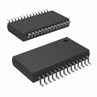
IC DESERIALIZER 10BIT 28-SSOP
Manufacturer
National Semiconductor
Datasheet
1.DS92LV1224TMSANOPB.pdf
(13 pages)
Specifications of DS92LV1224TMSAX/NOPB
Function
Deserializer
Data Rate
660Mbps
Input Type
LVDS
Output Type
LVTTL
Number Of Inputs
1
Number Of Outputs
10
Voltage - Supply
3 V ~ 3.6 V
Operating Temperature
-40°C ~ 85°C
Mounting Type
Surface Mount
Package / Case
28-SSOP
Lead Free Status / RoHS Status
Lead free / RoHS Compliant
Other names
*DS92LV1224TMSAX
DS92LV1224TMSAX
DS92LV1224TMSAX
Available stocks
Company
Part Number
Manufacturer
Quantity
Price
Company:

Part Number:
DS92LV1224TMSAX/NOPB
Manufacturer:
NS
Quantity:
14 052


SERIALIZER LVCMOS/LVTTL DC SPECIFICATIONS (apply to DIN0-9, TCLK, PWRDN, TCLK_R/F, SYNC1, SYNC2, DEN)
V
V
V
I
SERIALIZER Bus LVDS DC SPECIFICATIONS (apply to pins DO+ and DO−)
V
∆V
V
∆V
I
I
I
SERIALIZER SUPPLY CURRENT (apply to pins DVCC and AVCC)
I
I
IN
OS
OZ
OX
CCD
CCXD
IH
IL
CL
OD
OS
Absolute Maximum Ratings
If Military/Aerospace specified devices are required,
please contact the National Semiconductor Sales Office/
Distributors for availability and specifications.
Electrical Characteristics
Over recommended operating supply and temperature ranges unless otherwise specified.
Symbol
OD
OS
Supply Voltage (V
LVCMOS/LVTTL Input
Voltage
LVCMOS/LVTTL Output
Voltage
Bus LVDS Driver Output
Voltage
Bus LVDS Output Short
Circuit
Junction Temperature
Storage Temperature
Lead Temperature
Maximum Package Power Dissipation Capacity
@
(Soldering, 4 seconds)
28L SSOP
25˚C Package:
High Level Input Voltage
Low Level Input Voltage
Input Clamp Voltage
Input Current
Output Differential Voltage
(DO+)–(DO−)
Output Differential Voltage
Unbalance
Offset Voltage
Offset Voltage Unbalance
Output Short Circuit Current
TRI-STATE Output Current
Power-Off Output Current
Serializer Supply Current
Worst Case
Serializer Supply Current Powerdown PWRDN = 0.8V
Duration
CC
Parameter
)
−0.3V to (V
−0.3V to (V
−65˚C to +150˚C
−0.3V to +3.9V
−0.3V to +4V
CC
CC
(Note 1)
+150˚C
+260˚C
1.27 W
+0.3V)
+0.3V)
10mS
I
V
RL = 27Ω, Figure 10
D0 = 0V, DIN = High,PWRDN and DEN =
2.4V
PWRDN or DEN = 0.8V, DO = 0V or VCC
VCC = 0V, DO=0V or 3.6V
RL = 27Ω
Figure 2
CL
IN
= −18 mA
= 0V or 3.6V
5
Recommended Operating
Conditions
Conditions
Supply Voltage (V
Operating Free Air
Supply Noise Voltage
Temperature (T
(V
Package Derating:
28L SSOP
θ
θ
ESD Rating
CC
ja
jc
HBM (1.5kOhm, 100pF)
MM
)
f = 40 MHz
f = 66 MHz
A
CC
)
)
GND
Min
−40
1.05
Min
−10
−10
−20
3.0
200
2.0
10.3 mW/˚C above
Nom
+25
3.3
-0.86
Typ
−56
290
1.1
4.8
±
±
±
47
75
47
1
1
1
Max
+85
3.6
97˚C/W
27˚C/W
>
−1.5
Max
V
+10
−90
+10
+25
100 mV
500
www.national.com
0.8
1.3
+25˚C
35
35
60
90
>
CC
250V
1kV
Units
˚C
V
Units
P-P
mV
mV
mV
mA
mA
mA
µA
µA
µA
µA
V
V
V
V
Related parts for DS92LV1224TMSAX/NOPB
Image
Part Number
Description
Manufacturer
Datasheet
Request
R

Part Number:
Description:
National Semiconductor [8-Bit D/A Converter]
Manufacturer:
National Semiconductor
Datasheet:
Part Number:
Description:
National Semiconductor [Media Coprocessor]
Manufacturer:
National Semiconductor
Datasheet:
Part Number:
Description:
Digitally Controlled Tone and Volume Circuit with Stereo Audio Power Amplifier, Microphone Preamp Stage and National 3D Sound
Manufacturer:
National Semiconductor
Datasheet:
Part Number:
Description:
Digitally Controlled Tone and Volume Circuit with Stereo Audio Power Amplifier, Microphone Preamp Stage and National 3D Sound
Manufacturer:
National Semiconductor
Datasheet:
Part Number:
Description:
AC97 Rev 2 Codec with Sample Rate Conversion and National 3D Sound
Manufacturer:
National Semiconductor
Part Number:
Description:
Manufacturer:
National Semiconductor
Datasheet:
Part Number:
Description:
Manufacturer:
National Semiconductor
Datasheet:
Part Number:
Description:
General Purpose, Low Voltage, Low Power, Rail-to-Rail Output Operational Amplifiers
Manufacturer:
National Semiconductor
Datasheet:
Part Number:
Description:
8-bit 20 MSPS flash A/D converter.
Manufacturer:
National Semiconductor
Datasheet:
Part Number:
Description:
Low Noise Quad Operational Amplifier
Manufacturer:
National Semiconductor
Datasheet:
Part Number:
Description:
Quad Differential Line Receivers
Manufacturer:
National Semiconductor
Datasheet:
Part Number:
Description:
Quad High Speed Trapezoidal? Bus Transceiver
Manufacturer:
National Semiconductor
Datasheet:
Part Number:
Description:
Dual Line Receiver
Manufacturer:
National Semiconductor
Datasheet:
Part Number:
Description:
TTL to 10k ECL Level Translator with Latch
Manufacturer:
National Semiconductor
Datasheet: